Download as PDF, PPTX
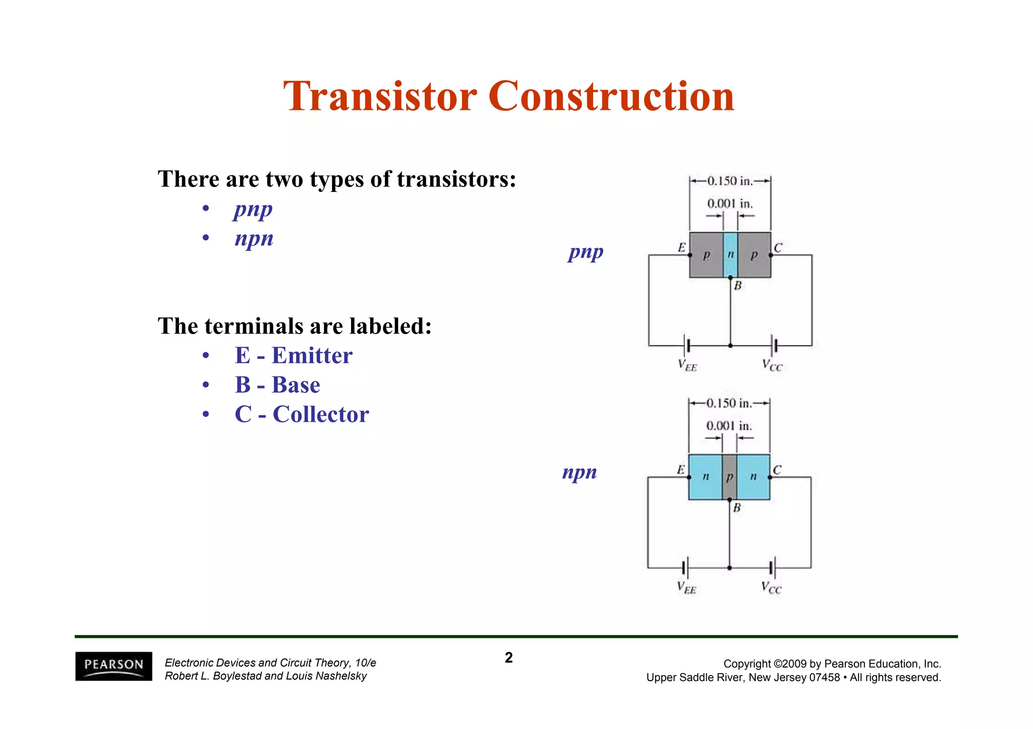
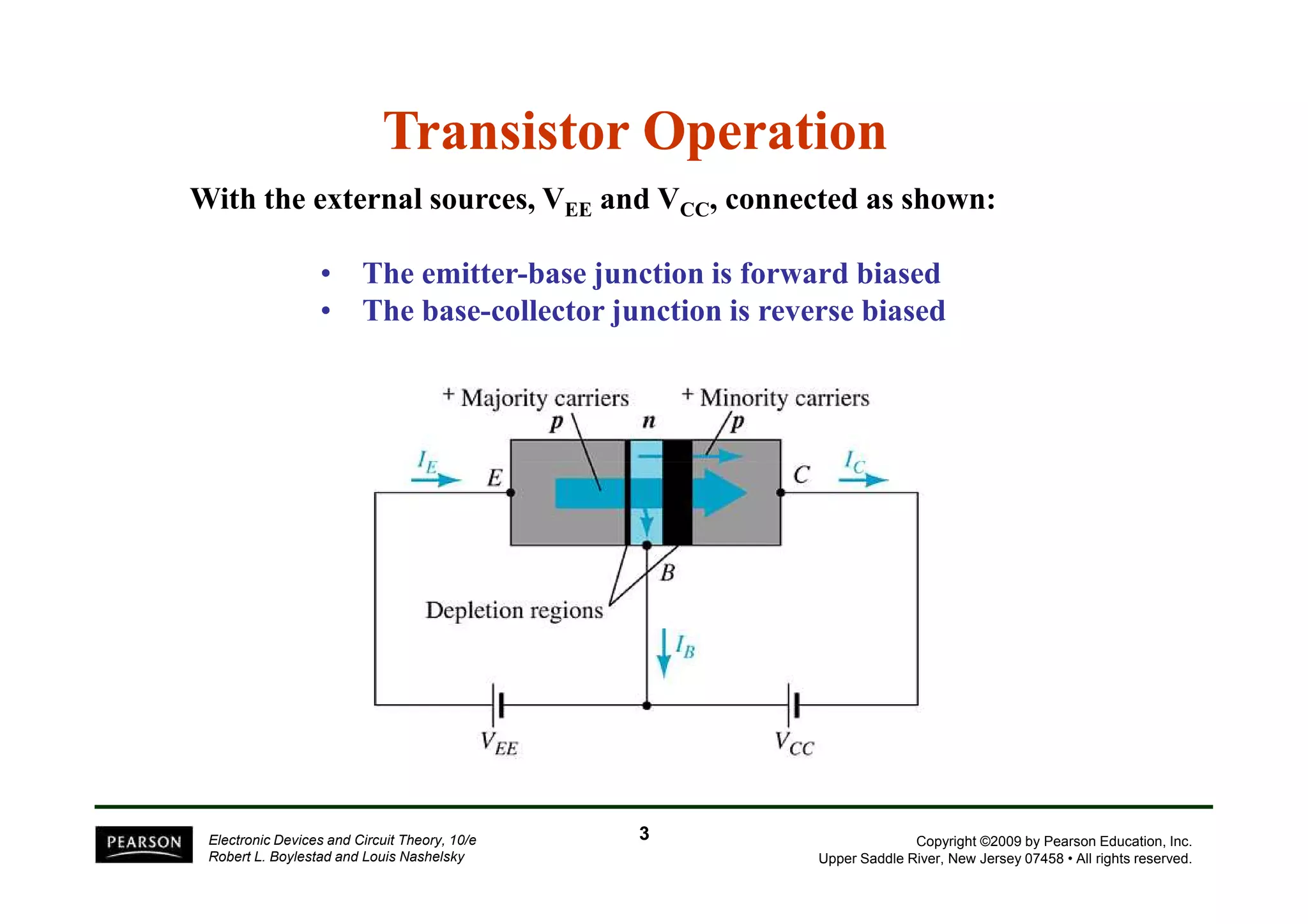
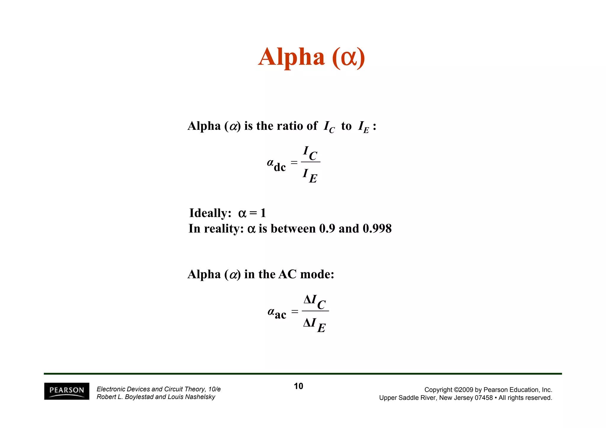
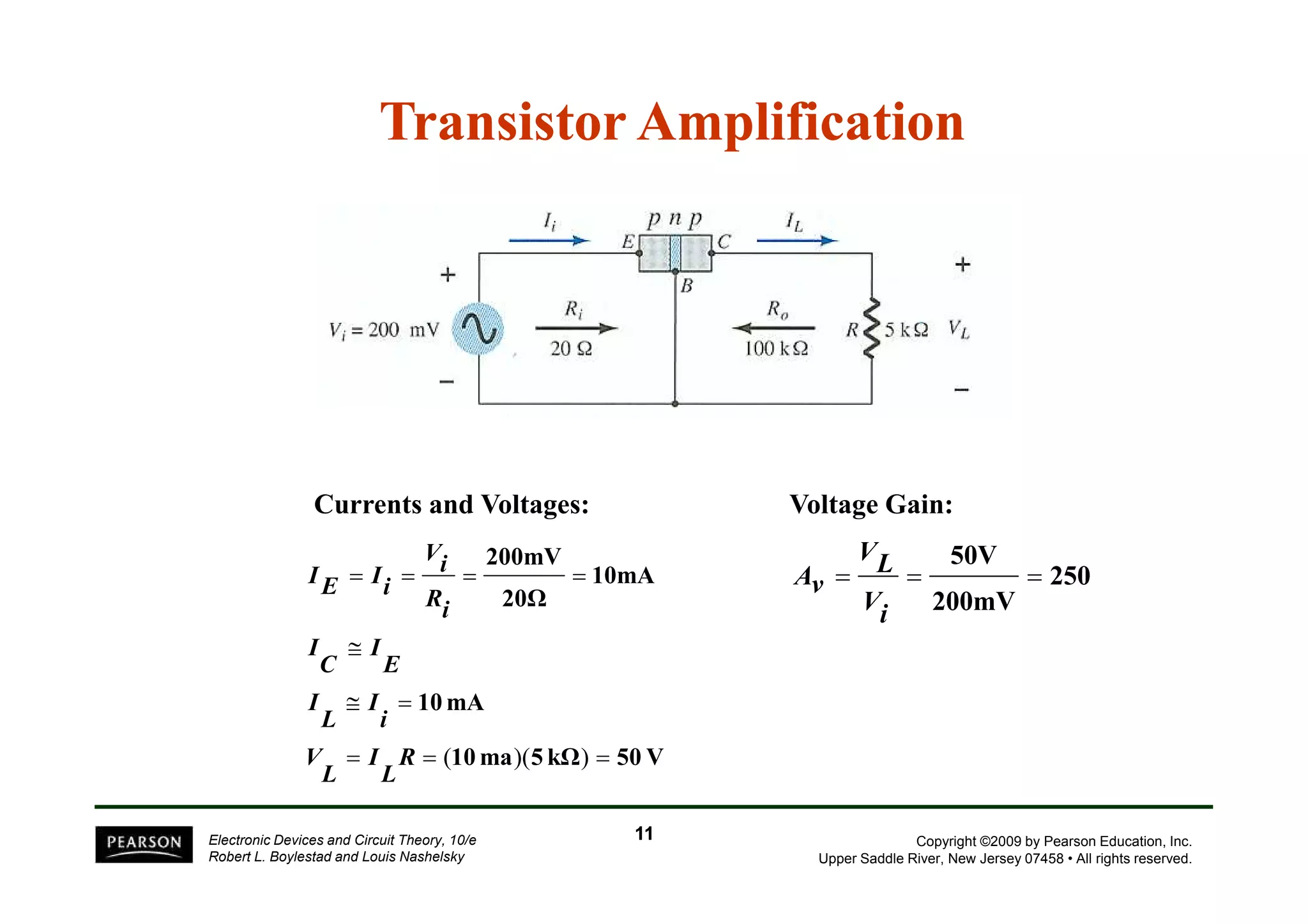
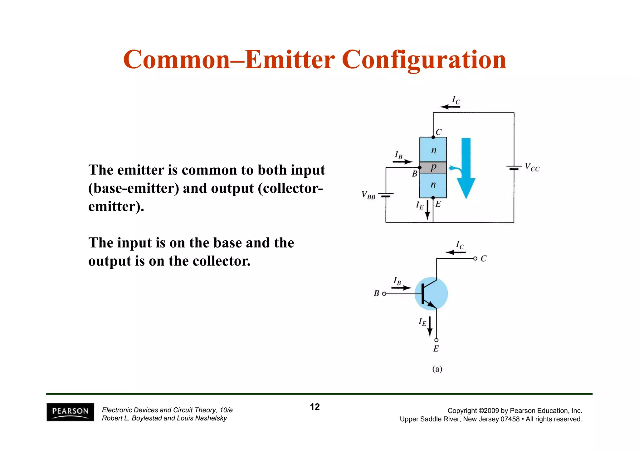
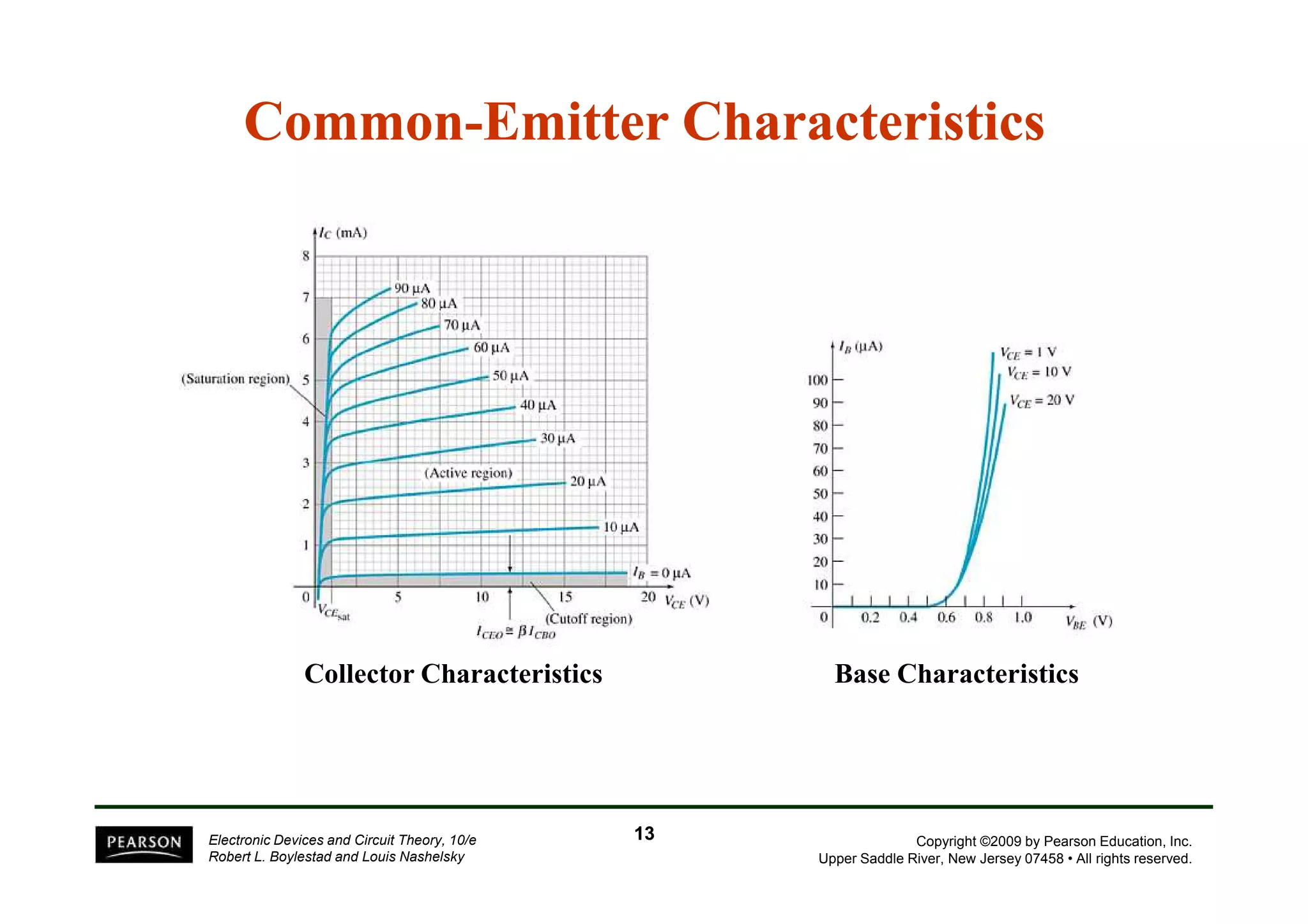
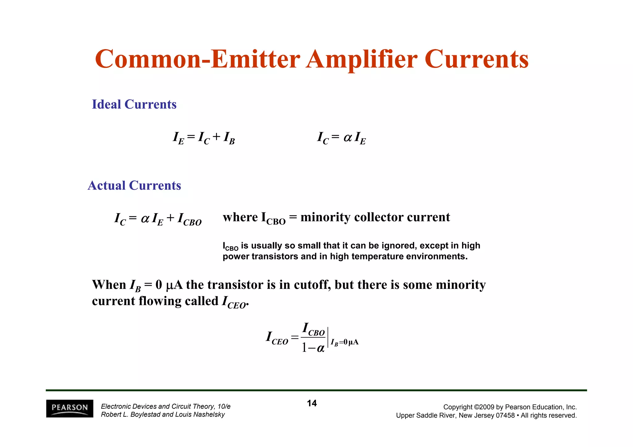
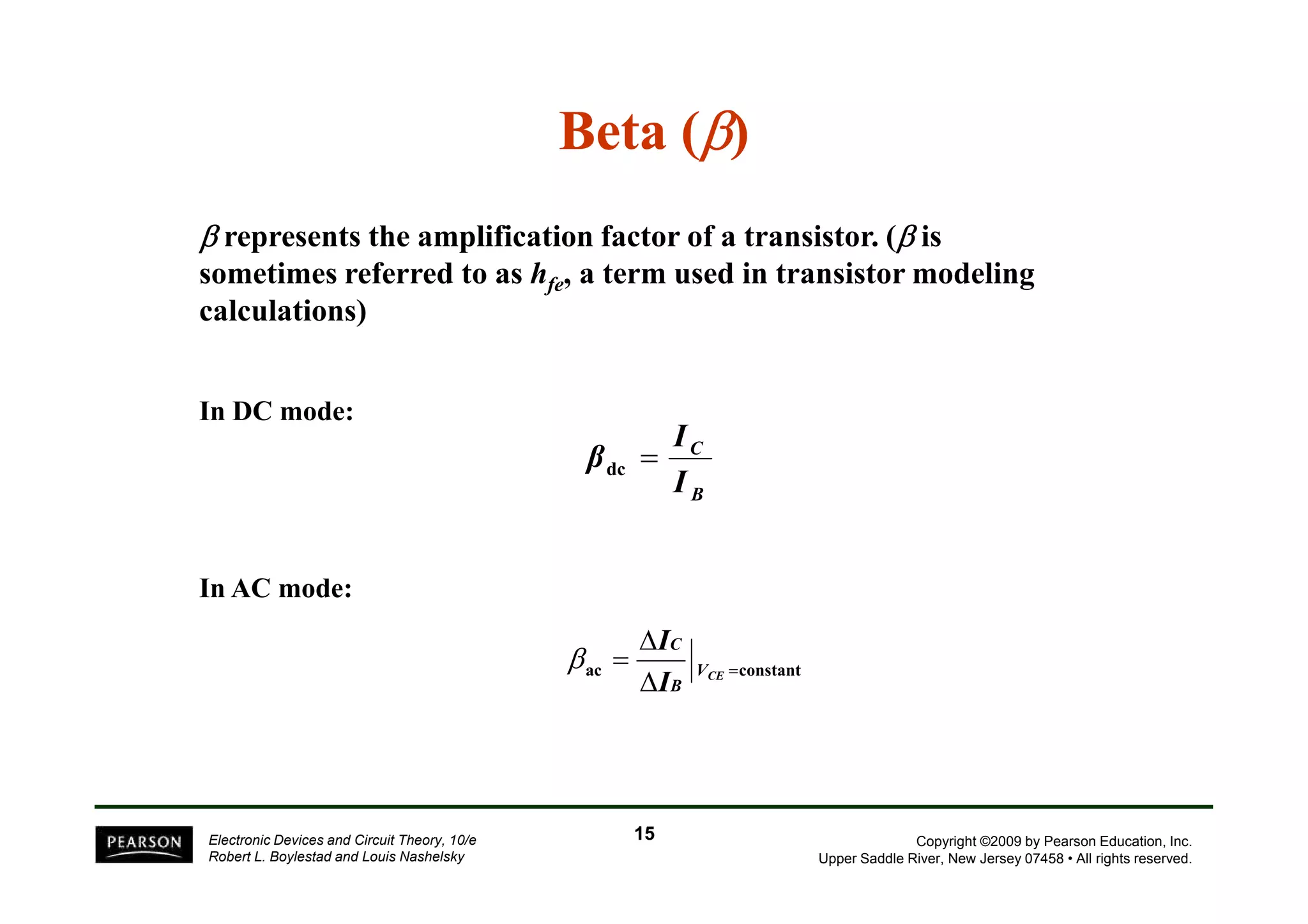
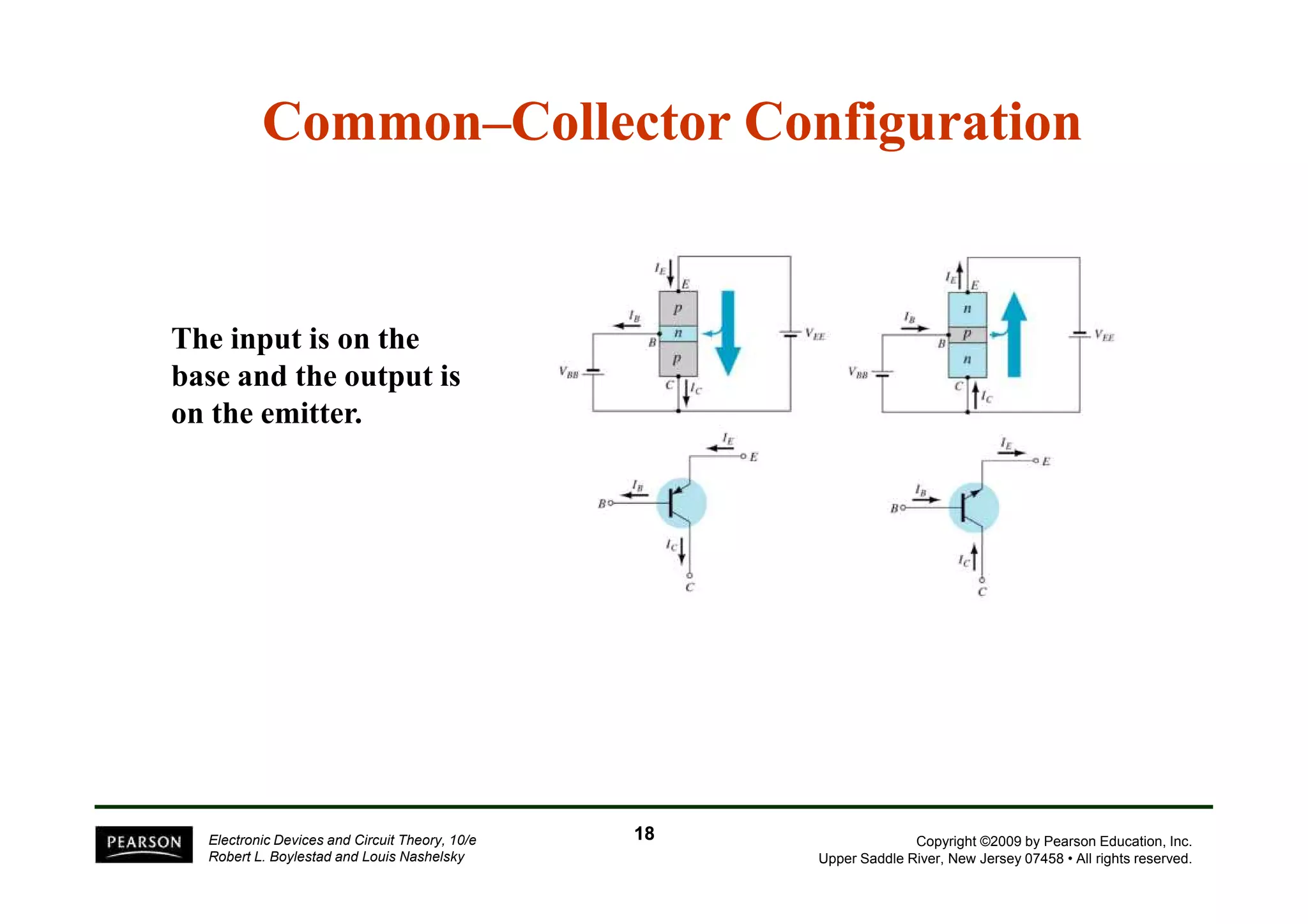
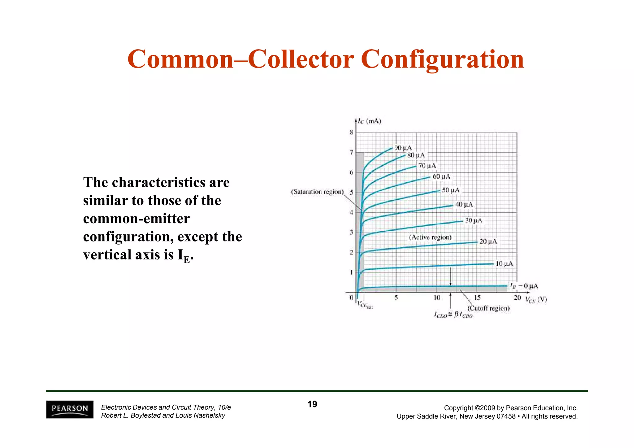
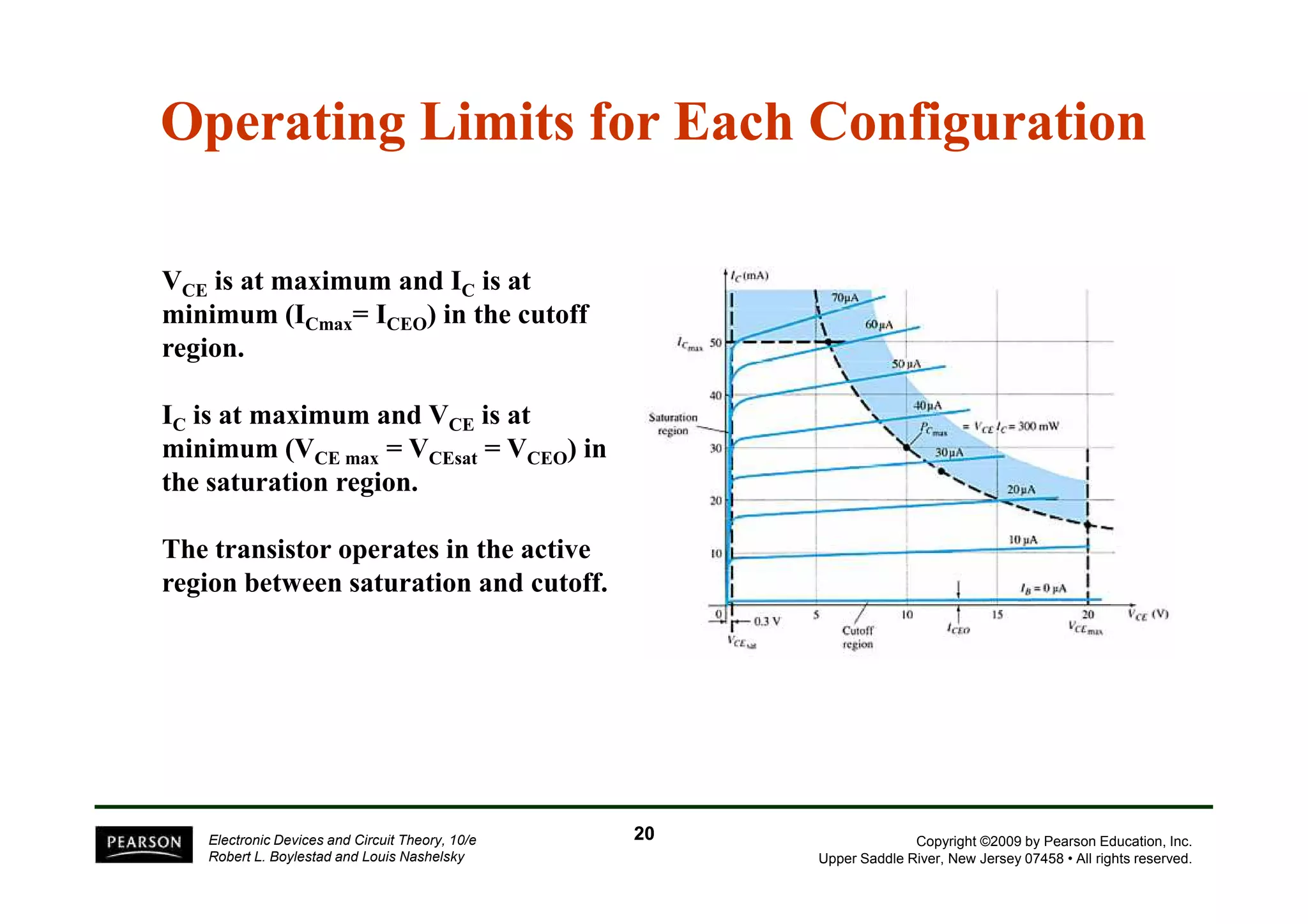
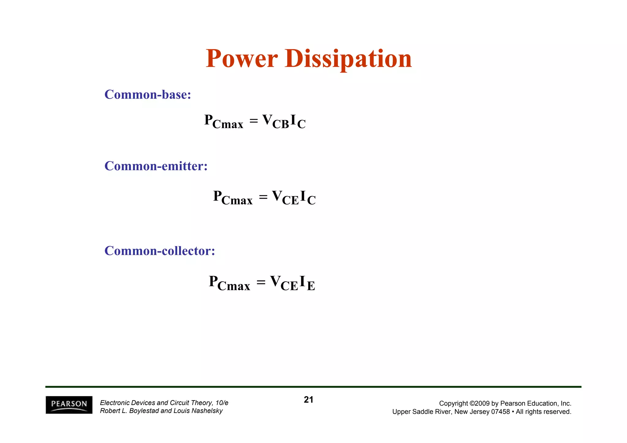
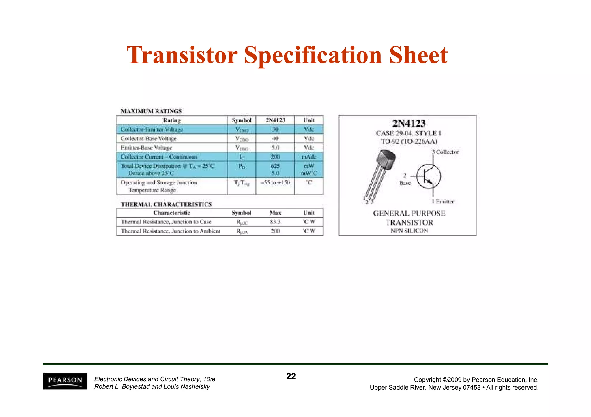
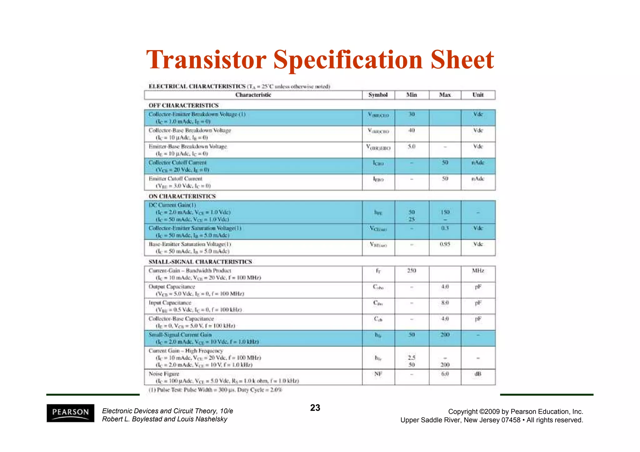

There are two types of transistors, PNP and NPN. A transistor has three terminals - emitter, base, and collector. In an NPN transistor, the emitter-base junction is forward biased and the base-collector junction is reverse biased. There are three common transistor configurations - common-base, common-emitter, and common-collector. The common-emitter configuration is most widely used. A transistor can be used to amplify signals and its gain is determined by its beta value. Transistors have defined operating regions and limits that depend on the configuration.