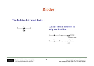
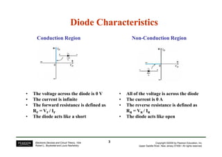
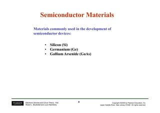
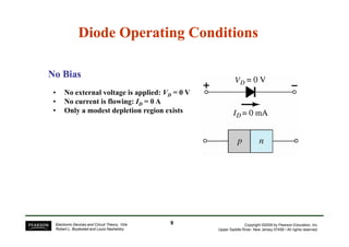
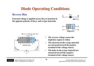
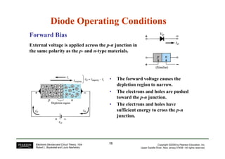
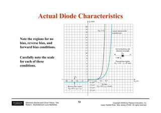
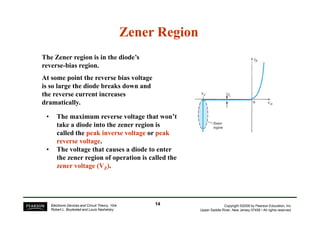
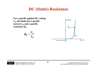
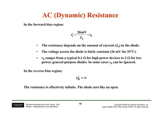
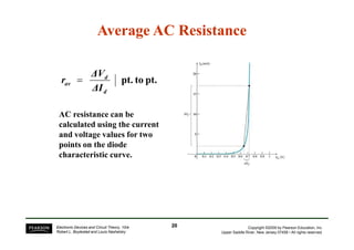
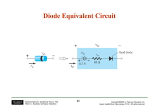
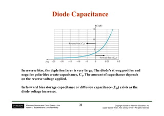
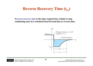
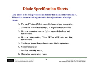
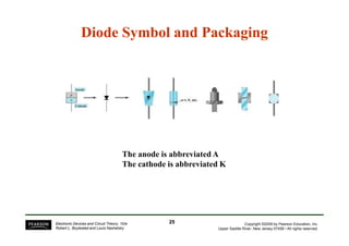
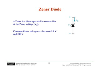
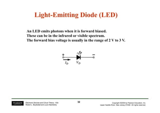
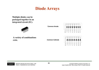
Chapter 1:
Semiconductor Diodes
Diodes
Diodes
The diode is a 2-terminal device.
A diode ideally conducts in
only one direction.
Copyright ©2009 by Pearson Education, Inc.
Upper Saddle River, New Jersey 07458 • All rights reserved.
Electronic Devices and Circuit Theory, 10/e
Robert L. Boylestad and Louis Nashelsky
2
2
Diode Characteristics
Conduction Region
Conduction Region Non
Non-
-Conduction Region
Conduction Region
Copyright ©2009 by Pearson Education, Inc.
Upper Saddle River, New Jersey 07458 • All rights reserved.
Electronic Devices and Circuit Theory, 10/e
Robert L. Boylestad and Louis Nashelsky
• The voltage across the diode is 0 V
• The current is infinite
• The forward resistance is defined as
RF = VF / IF
• The diode acts like a short
• All of the voltage is across the diode
• The current is 0 A
• The reverse resistance is defined as
RR = VR / IR
• The diode acts like open
3
3
Semiconductor Materials
Materials commonly used in the development of
semiconductor devices:
•
• Silicon (Si)
Silicon (Si)
•
• Germanium (Ge)
Germanium (Ge)
•
• Gallium Arsenide (GaAs)
Gallium Arsenide (GaAs)
Copyright ©2009 by Pearson Education, Inc.
Upper Saddle River, New Jersey 07458 • All rights reserved.
Electronic Devices and Circuit Theory, 10/e
Robert L. Boylestad and Louis Nashelsky
4
4
Doping
Doping
The electrical characteristics of silicon and germanium are improved
by adding materials in a process called doping.
There are just two types of doped semiconductor materials:
n
n-
-type
type
p
p-
-type
type
Copyright ©2009 by Pearson Education, Inc.
Upper Saddle River, New Jersey 07458 • All rights reserved.
Electronic Devices and Circuit Theory, 10/e
Robert L. Boylestad and Louis Nashelsky
p
p-
-type
type
• n-type materials contain an excess of conduction band electrons.
• p-type materials contain an excess of valence band holes.
5
5
p
p-
-n
n Junctions
Junctions
One end of a silicon or germanium crystal can be doped as a p-
type material and the other end as an n-type material.
The result is a p
p-
-n
n junction
junction.
Copyright ©2009 by Pearson Education, Inc.
Upper Saddle River, New Jersey 07458 • All rights reserved.
Electronic Devices and Circuit Theory, 10/e
Robert L. Boylestad and Louis Nashelsky
The result is a p
p-
-n
n junction
junction.
6
6
p
p-
-n
n Junctions
Junctions
At the p-n junction, the excess
conduction-band electrons on the
n-type side are attracted to the
valence-band holes on the p-type
side.
The electrons in the n-type
material migrate across the
junction to the p-type material
Copyright ©2009 by Pearson Education, Inc.
Upper Saddle River, New Jersey 07458 • All rights reserved.
Electronic Devices and Circuit Theory, 10/e
Robert L. Boylestad and Louis Nashelsky
junction to the p-type material
(electron flow).
The electron migration results in
a negative
negative charge on the p-type
side of the junction and a positive
positive
charge on the n-type side of the
junction.
The result is the formation of a
depletion region
depletion region around the
junction.
7
7
Diode Operating Conditions
A diode has three operating conditions:
• No bias
• Forward bias
• Reverse bias
Copyright ©2009 by Pearson Education, Inc.
Upper Saddle River, New Jersey 07458 • All rights reserved.
Electronic Devices and Circuit Theory, 10/e
Robert L. Boylestad and Louis Nashelsky
8
8
Diode Operating Conditions
• No external voltage is applied: VD = 0 V
• No current is flowing: ID = 0 A
• Only a modest depletion region exists
No Bias
No Bias
Copyright ©2009 by Pearson Education, Inc.
Upper Saddle River, New Jersey 07458 • All rights reserved.
Electronic Devices and Circuit Theory, 10/e
Robert L. Boylestad and Louis Nashelsky
9
9
External voltage is applied across the p-n junction in
the opposite polarity of the p- and n-type materials.
Diode Operating Conditions
Reverse Bias
Reverse Bias
Copyright ©2009 by Pearson Education, Inc.
Upper Saddle River, New Jersey 07458 • All rights reserved.
Electronic Devices and Circuit Theory, 10/e
Robert L. Boylestad and Louis Nashelsky
• The reverse voltage causes the
depletion region to widen.
• The electrons in the n-type material
are attracted toward the positive
terminal of the voltage source.
• The holes in the p-type material are
attracted toward the negative
terminal of the voltage source.
10
10
Diode Operating Conditions
Forward Bias
Forward Bias
External voltage is applied across the p-n junction in
the same polarity as the p- and n-type materials.
• The forward voltage causes the
Copyright ©2009 by Pearson Education, Inc.
Upper Saddle River, New Jersey 07458 • All rights reserved.
Electronic Devices and Circuit Theory, 10/e
Robert L. Boylestad and Louis Nashelsky
• The forward voltage causes the
depletion region to narrow.
• The electrons and holes are pushed
toward the p-n junction.
• The electrons and holes have
sufficient energy to cross the p-n
junction.
11
11
Actual Diode Characteristics
Note the regions for no
bias, reverse bias, and
forward bias conditions.
Carefully note the scale
Copyright ©2009 by Pearson Education, Inc.
Upper Saddle River, New Jersey 07458 • All rights reserved.
Electronic Devices and Circuit Theory, 10/e
Robert L. Boylestad and Louis Nashelsky
Carefully note the scale
for each of these
conditions.
12
12
Two currents through a diode:
Majority and Minority Carriers
Majority Carriers
Majority Carriers
• The majority carriers in n-type materials are electrons.
• The majority carriers in p-type materials are holes.
Copyright ©2009 by Pearson Education, Inc.
Upper Saddle River, New Jersey 07458 • All rights reserved.
Electronic Devices and Circuit Theory, 10/e
Robert L. Boylestad and Louis Nashelsky
Minority Carriers
Minority Carriers
• The minority carriers in n-type materials are holes.
• The minority carriers in p-type materials are electrons.
13
13
The Zener region is in the diode’s
reverse-bias region.
At some point the reverse bias voltage
is so large the diode breaks down and
the reverse current increases
dramatically.
Zener Region
Zener Region
• The maximum reverse voltage that won’t
Copyright ©2009 by Pearson Education, Inc.
Upper Saddle River, New Jersey 07458 • All rights reserved.
Electronic Devices and Circuit Theory, 10/e
Robert L. Boylestad and Louis Nashelsky
• The maximum reverse voltage that won’t
take a diode into the zener region is
called the peak inverse voltage
peak inverse voltage or peak
peak
reverse voltage
reverse voltage.
• The voltage that causes a diode to enter
the zener region of operation is called the
zener voltage (V
zener voltage (VZ
Z)
).
14
14
The point at which the diode changes from no-bias condition
to forward-bias condition occurs when the electrons and
holes are given sufficient energy to cross the p-n junction.
This energy comes from the external voltage applied across
the diode.
Forward Bias Voltage
The forward bias voltage required for a:
Copyright ©2009 by Pearson Education, Inc.
Upper Saddle River, New Jersey 07458 • All rights reserved.
Electronic Devices and Circuit Theory, 10/e
Robert L. Boylestad and Louis Nashelsky
The forward bias voltage required for a:
• gallium arsenide diode ≅
≅
≅
≅ 1.2 V
• silicon diode ≅
≅
≅
≅ 0.7 V
• germanium diode ≅
≅
≅
≅ 0.3 V
15
15
As temperature increases it adds energy to the diode.
• It reduces the required forward bias voltage for forward-
bias conduction.
• It increases the amount of reverse current in the reverse-
bias condition.
Temperature Effects
Temperature Effects
Copyright ©2009 by Pearson Education, Inc.
Upper Saddle River, New Jersey 07458 • All rights reserved.
Electronic Devices and Circuit Theory, 10/e
Robert L. Boylestad and Louis Nashelsky
• It increases maximum reverse bias avalanche voltage.
Germanium diodes are more sensitive to temperature
variations than silicon or gallium arsenide diodes.
16
16
Semiconductors react differently to DC and AC currents.
There are three types of resistance:
• DC (static) resistance
• AC (dynamic) resistance
Resistance Levels
Resistance Levels
Copyright ©2009 by Pearson Education, Inc.
Upper Saddle River, New Jersey 07458 • All rights reserved.
Electronic Devices and Circuit Theory, 10/e
Robert L. Boylestad and Louis Nashelsky
• AC (dynamic) resistance
• Average AC resistance
17
17
DC (Static) Resistance
For a specific applied DC voltage
VD, the diode has a specific
current ID, and a specific
resistance RD.
D
D
V
R =
Copyright ©2009 by Pearson Education, Inc.
Upper Saddle River, New Jersey 07458 • All rights reserved.
Electronic Devices and Circuit Theory, 10/e
Robert L. Boylestad and Louis Nashelsky
D
D
I
R =
18
18
• The resistance depends on the amount of current (ID) in the diode.
• The voltage across the diode is fairly constant (26 mV for 25°
°
°
°C).
• r ranges from a typical 0.1 Ω
Ω
Ω
Ω for high power devices to 2 Ω
Ω
Ω
Ω for low
AC (Dynamic) Resistance
B
D
d r
I
r +
=
′
mV
26
In the forward bias region:
Copyright ©2009 by Pearson Education, Inc.
Upper Saddle River, New Jersey 07458 • All rights reserved.
Electronic Devices and Circuit Theory, 10/e
Robert L. Boylestad and Louis Nashelsky
• rB ranges from a typical 0.1 Ω
Ω
Ω
Ω for high power devices to 2 Ω
Ω
Ω
Ω for low
power, general purpose diodes. In some cases rB can be ignored.
∞
∞
∞
∞
=
=
=
=
′
′
′
′
rd
In the reverse bias region:
The resistance is effectively infinite. The diode acts like an open.
19
19
AC resistance can be
calculated using the current
Average AC Resistance
pt.
to
pt.
d
d
av
∆I
∆V
r =
Copyright ©2009 by Pearson Education, Inc.
Upper Saddle River, New Jersey 07458 • All rights reserved.
Electronic Devices and Circuit Theory, 10/e
Robert L. Boylestad and Louis Nashelsky
calculated using the current
and voltage values for two
points on the diode
characteristic curve.
20
20
Diode Equivalent Circuit
Copyright ©2009 by Pearson Education, Inc.
Upper Saddle River, New Jersey 07458 • All rights reserved.
Electronic Devices and Circuit Theory, 10/e
Robert L. Boylestad and Louis Nashelsky
21
21
Diode Capacitance
Diode Capacitance
Copyright ©2009 by Pearson Education, Inc.
Upper Saddle River, New Jersey 07458 • All rights reserved.
Electronic Devices and Circuit Theory, 10/e
Robert L. Boylestad and Louis Nashelsky
In reverse bias, the depletion layer is very large. The diode’s strong positive and
negative polarities create capacitance, CT. The amount of capacitance depends
on the reverse voltage applied.
In forward bias storage capacitance or diffusion capacitance (CD) exists as the
diode voltage increases.
22
22
Reverse recovery time
Reverse recovery time is the time required for a diode to stop
conducting once it is switched from forward bias to reverse bias.
Reverse Recovery Time (t
Reverse Recovery Time (trr
rr)
)
Copyright ©2009 by Pearson Education, Inc.
Upper Saddle River, New Jersey 07458 • All rights reserved.
Electronic Devices and Circuit Theory, 10/e
Robert L. Boylestad and Louis Nashelsky
23
23
1. Forward Voltage (VF) at a specified current and temperature
2. Maximum forward current (IF) at a specified temperature
3. Reverse saturation current (IR) at a specified voltage and
temperature
Diode Specification Sheets
Data about a diode is presented uniformly for many different diodes.
This makes cross-matching of diodes for replacement or design
easier.
Copyright ©2009 by Pearson Education, Inc.
Upper Saddle River, New Jersey 07458 • All rights reserved.
Electronic Devices and Circuit Theory, 10/e
Robert L. Boylestad and Louis Nashelsky
temperature
4. Reverse voltage rating, PIV or PRV or V(BR), at a specified
temperature
5. Maximum power dissipation at a specified temperature
6. Capacitance levels
7. Reverse recovery time, trr
8. Operating temperature range
24
24
Diode Symbol and Packaging
Copyright ©2009 by Pearson Education, Inc.
Upper Saddle River, New Jersey 07458 • All rights reserved.
Electronic Devices and Circuit Theory, 10/e
Robert L. Boylestad and Louis Nashelsky
The anode is abbreviated A
The cathode is abbreviated K
25
25
Diode Testing
Diode Testing
Diode checker
Ohmmeter
Curve tracer
Copyright ©2009 by Pearson Education, Inc.
Upper Saddle River, New Jersey 07458 • All rights reserved.
Electronic Devices and Circuit Theory, 10/e
Robert L. Boylestad and Louis Nashelsky
26
26
Diode Checker
Diode Checker
• Gallium arsenide ≅
≅
≅
≅ 1.2 V
Many digital multimeters have a diode checking function.
The diode should be tested out of circuit.
A normal diode exhibits its forward voltage:
Copyright ©2009 by Pearson Education, Inc.
Upper Saddle River, New Jersey 07458 • All rights reserved.
Electronic Devices and Circuit Theory, 10/e
Robert L. Boylestad and Louis Nashelsky
• Gallium arsenide ≅
≅
≅
≅ 1.2 V
• Silicon diode ≅
≅
≅
≅ 0.7 V
• Germanium diode ≅
≅
≅
≅ 0.3 V
27
27
An ohmmeter set on a low Ohms scale can be used to test a
diode. The diode should be tested out of circuit.
Ohmmeter
Ohmmeter
Copyright ©2009 by Pearson Education, Inc.
Upper Saddle River, New Jersey 07458 • All rights reserved.
Electronic Devices and Circuit Theory, 10/e
Robert L. Boylestad and Louis Nashelsky
28
28
Curve Tracer
Curve Tracer
A curve tracer displays the characteristic curve of a diode in the
test circuit. This curve can be compared to the specifications of
the diode from a data sheet.
Copyright ©2009 by Pearson Education, Inc.
Upper Saddle River, New Jersey 07458 • All rights reserved.
Electronic Devices and Circuit Theory, 10/e
Robert L. Boylestad and Louis Nashelsky
29
29
Other Types of Diodes
Zener diode
Light-emitting diode
Diode arrays
Copyright ©2009 by Pearson Education, Inc.
Upper Saddle River, New Jersey 07458 • All rights reserved.
Electronic Devices and Circuit Theory, 10/e
Robert L. Boylestad and Louis Nashelsky
30
30
A Zener is a diode operated in reverse bias
at the Zener voltage (VZ).
Common Zener voltages are between 1.8 V
and 200 V
Zener Diode
Zener Diode
Copyright ©2009 by Pearson Education, Inc.
Upper Saddle River, New Jersey 07458 • All rights reserved.
Electronic Devices and Circuit Theory, 10/e
Robert L. Boylestad and Louis Nashelsky
and 200 V
31
31
Light
Light-
-Emitting Diode (LED)
Emitting Diode (LED)
An LED emits photons when it is forward biased.
These can be in the infrared or visible spectrum.
The forward bias voltage is usually in the range of 2 V to 3 V.
Copyright ©2009 by Pearson Education, Inc.
Upper Saddle River, New Jersey 07458 • All rights reserved.
Electronic Devices and Circuit Theory, 10/e
Robert L. Boylestad and Louis Nashelsky
32
32
Multiple diodes can be
packaged together in an
integrated circuit (IC).
Common Anode
Common Anode
Diode Arrays
Diode Arrays
Copyright ©2009 by Pearson Education, Inc.
Upper Saddle River, New Jersey 07458 • All rights reserved.
Electronic Devices and Circuit Theory, 10/e
Robert L. Boylestad and Louis Nashelsky
Common Cathode
Common Cathode
A variety of combinations
exist.
33
33

Bem (3)

  • 1.
  • 2.
    Diodes Diodes The diode isa 2-terminal device. A diode ideally conducts in only one direction. Copyright ©2009 by Pearson Education, Inc. Upper Saddle River, New Jersey 07458 • All rights reserved. Electronic Devices and Circuit Theory, 10/e Robert L. Boylestad and Louis Nashelsky 2 2
  • 3.
    Diode Characteristics Diode Characteristics ConductionRegion Conduction Region Non Non- -Conduction Region Conduction Region Copyright ©2009 by Pearson Education, Inc. Upper Saddle River, New Jersey 07458 • All rights reserved. Electronic Devices and Circuit Theory, 10/e Robert L. Boylestad and Louis Nashelsky • The voltage across the diode is 0 V • The current is infinite • The forward resistance is defined as RF = VF / IF • The diode acts like a short • All of the voltage is across the diode • The current is 0 A • The reverse resistance is defined as RR = VR / IR • The diode acts like open 3 3
  • 4.
    Semiconductor Materials Semiconductor Materials Materialscommonly used in the development of semiconductor devices: • • Silicon (Si) Silicon (Si) • • Germanium (Ge) Germanium (Ge) • • Gallium Arsenide (GaAs) Gallium Arsenide (GaAs) Copyright ©2009 by Pearson Education, Inc. Upper Saddle River, New Jersey 07458 • All rights reserved. Electronic Devices and Circuit Theory, 10/e Robert L. Boylestad and Louis Nashelsky 4 4
  • 5.
    Doping Doping The electrical characteristicsof silicon and germanium are improved by adding materials in a process called doping. There are just two types of doped semiconductor materials: n n- -type type p p- -type type Copyright ©2009 by Pearson Education, Inc. Upper Saddle River, New Jersey 07458 • All rights reserved. Electronic Devices and Circuit Theory, 10/e Robert L. Boylestad and Louis Nashelsky p p- -type type • n-type materials contain an excess of conduction band electrons. • p-type materials contain an excess of valence band holes. 5 5
  • 6.
    p p- -n n Junctions Junctions One endof a silicon or germanium crystal can be doped as a p- type material and the other end as an n-type material. The result is a p p- -n n junction junction. Copyright ©2009 by Pearson Education, Inc. Upper Saddle River, New Jersey 07458 • All rights reserved. Electronic Devices and Circuit Theory, 10/e Robert L. Boylestad and Louis Nashelsky The result is a p p- -n n junction junction. 6 6
  • 7.
    p p- -n n Junctions Junctions At thep-n junction, the excess conduction-band electrons on the n-type side are attracted to the valence-band holes on the p-type side. The electrons in the n-type material migrate across the junction to the p-type material Copyright ©2009 by Pearson Education, Inc. Upper Saddle River, New Jersey 07458 • All rights reserved. Electronic Devices and Circuit Theory, 10/e Robert L. Boylestad and Louis Nashelsky junction to the p-type material (electron flow). The electron migration results in a negative negative charge on the p-type side of the junction and a positive positive charge on the n-type side of the junction. The result is the formation of a depletion region depletion region around the junction. 7 7
  • 8.
    Diode Operating Conditions DiodeOperating Conditions A diode has three operating conditions: • No bias • Forward bias • Reverse bias Copyright ©2009 by Pearson Education, Inc. Upper Saddle River, New Jersey 07458 • All rights reserved. Electronic Devices and Circuit Theory, 10/e Robert L. Boylestad and Louis Nashelsky 8 8
  • 9.
    Diode Operating Conditions DiodeOperating Conditions • No external voltage is applied: VD = 0 V • No current is flowing: ID = 0 A • Only a modest depletion region exists No Bias No Bias Copyright ©2009 by Pearson Education, Inc. Upper Saddle River, New Jersey 07458 • All rights reserved. Electronic Devices and Circuit Theory, 10/e Robert L. Boylestad and Louis Nashelsky 9 9
  • 10.
    External voltage isapplied across the p-n junction in the opposite polarity of the p- and n-type materials. Diode Operating Conditions Diode Operating Conditions Reverse Bias Reverse Bias Copyright ©2009 by Pearson Education, Inc. Upper Saddle River, New Jersey 07458 • All rights reserved. Electronic Devices and Circuit Theory, 10/e Robert L. Boylestad and Louis Nashelsky • The reverse voltage causes the depletion region to widen. • The electrons in the n-type material are attracted toward the positive terminal of the voltage source. • The holes in the p-type material are attracted toward the negative terminal of the voltage source. 10 10
  • 11.
    Diode Operating Conditions DiodeOperating Conditions Forward Bias Forward Bias External voltage is applied across the p-n junction in the same polarity as the p- and n-type materials. • The forward voltage causes the Copyright ©2009 by Pearson Education, Inc. Upper Saddle River, New Jersey 07458 • All rights reserved. Electronic Devices and Circuit Theory, 10/e Robert L. Boylestad and Louis Nashelsky • The forward voltage causes the depletion region to narrow. • The electrons and holes are pushed toward the p-n junction. • The electrons and holes have sufficient energy to cross the p-n junction. 11 11
  • 12.
    Actual Diode Characteristics ActualDiode Characteristics Note the regions for no bias, reverse bias, and forward bias conditions. Carefully note the scale Copyright ©2009 by Pearson Education, Inc. Upper Saddle River, New Jersey 07458 • All rights reserved. Electronic Devices and Circuit Theory, 10/e Robert L. Boylestad and Louis Nashelsky Carefully note the scale for each of these conditions. 12 12
  • 13.
    Two currents througha diode: Majority and Minority Carriers Majority and Minority Carriers Majority Carriers Majority Carriers • The majority carriers in n-type materials are electrons. • The majority carriers in p-type materials are holes. Copyright ©2009 by Pearson Education, Inc. Upper Saddle River, New Jersey 07458 • All rights reserved. Electronic Devices and Circuit Theory, 10/e Robert L. Boylestad and Louis Nashelsky Minority Carriers Minority Carriers • The minority carriers in n-type materials are holes. • The minority carriers in p-type materials are electrons. 13 13
  • 14.
    The Zener regionis in the diode’s reverse-bias region. At some point the reverse bias voltage is so large the diode breaks down and the reverse current increases dramatically. Zener Region Zener Region • The maximum reverse voltage that won’t Copyright ©2009 by Pearson Education, Inc. Upper Saddle River, New Jersey 07458 • All rights reserved. Electronic Devices and Circuit Theory, 10/e Robert L. Boylestad and Louis Nashelsky • The maximum reverse voltage that won’t take a diode into the zener region is called the peak inverse voltage peak inverse voltage or peak peak reverse voltage reverse voltage. • The voltage that causes a diode to enter the zener region of operation is called the zener voltage (V zener voltage (VZ Z) ). 14 14
  • 15.
    The point atwhich the diode changes from no-bias condition to forward-bias condition occurs when the electrons and holes are given sufficient energy to cross the p-n junction. This energy comes from the external voltage applied across the diode. Forward Bias Voltage Forward Bias Voltage The forward bias voltage required for a: Copyright ©2009 by Pearson Education, Inc. Upper Saddle River, New Jersey 07458 • All rights reserved. Electronic Devices and Circuit Theory, 10/e Robert L. Boylestad and Louis Nashelsky The forward bias voltage required for a: • gallium arsenide diode ≅ ≅ ≅ ≅ 1.2 V • silicon diode ≅ ≅ ≅ ≅ 0.7 V • germanium diode ≅ ≅ ≅ ≅ 0.3 V 15 15
  • 16.
    As temperature increasesit adds energy to the diode. • It reduces the required forward bias voltage for forward- bias conduction. • It increases the amount of reverse current in the reverse- bias condition. Temperature Effects Temperature Effects Copyright ©2009 by Pearson Education, Inc. Upper Saddle River, New Jersey 07458 • All rights reserved. Electronic Devices and Circuit Theory, 10/e Robert L. Boylestad and Louis Nashelsky • It increases maximum reverse bias avalanche voltage. Germanium diodes are more sensitive to temperature variations than silicon or gallium arsenide diodes. 16 16
  • 17.
    Semiconductors react differentlyto DC and AC currents. There are three types of resistance: • DC (static) resistance • AC (dynamic) resistance Resistance Levels Resistance Levels Copyright ©2009 by Pearson Education, Inc. Upper Saddle River, New Jersey 07458 • All rights reserved. Electronic Devices and Circuit Theory, 10/e Robert L. Boylestad and Louis Nashelsky • AC (dynamic) resistance • Average AC resistance 17 17
  • 18.
    DC (Static) Resistance DC(Static) Resistance For a specific applied DC voltage VD, the diode has a specific current ID, and a specific resistance RD. D D V R = Copyright ©2009 by Pearson Education, Inc. Upper Saddle River, New Jersey 07458 • All rights reserved. Electronic Devices and Circuit Theory, 10/e Robert L. Boylestad and Louis Nashelsky D D I R = 18 18
  • 19.
    • The resistancedepends on the amount of current (ID) in the diode. • The voltage across the diode is fairly constant (26 mV for 25° ° ° °C). • r ranges from a typical 0.1 Ω Ω Ω Ω for high power devices to 2 Ω Ω Ω Ω for low AC (Dynamic) Resistance AC (Dynamic) Resistance B D d r I r + = ′ mV 26 In the forward bias region: Copyright ©2009 by Pearson Education, Inc. Upper Saddle River, New Jersey 07458 • All rights reserved. Electronic Devices and Circuit Theory, 10/e Robert L. Boylestad and Louis Nashelsky • rB ranges from a typical 0.1 Ω Ω Ω Ω for high power devices to 2 Ω Ω Ω Ω for low power, general purpose diodes. In some cases rB can be ignored. ∞ ∞ ∞ ∞ = = = = ′ ′ ′ ′ rd In the reverse bias region: The resistance is effectively infinite. The diode acts like an open. 19 19
  • 20.
    AC resistance canbe calculated using the current Average AC Resistance Average AC Resistance pt. to pt. d d av ∆I ∆V r = Copyright ©2009 by Pearson Education, Inc. Upper Saddle River, New Jersey 07458 • All rights reserved. Electronic Devices and Circuit Theory, 10/e Robert L. Boylestad and Louis Nashelsky calculated using the current and voltage values for two points on the diode characteristic curve. 20 20
  • 21.
    Diode Equivalent Circuit DiodeEquivalent Circuit Copyright ©2009 by Pearson Education, Inc. Upper Saddle River, New Jersey 07458 • All rights reserved. Electronic Devices and Circuit Theory, 10/e Robert L. Boylestad and Louis Nashelsky 21 21
  • 22.
    Diode Capacitance Diode Capacitance Copyright©2009 by Pearson Education, Inc. Upper Saddle River, New Jersey 07458 • All rights reserved. Electronic Devices and Circuit Theory, 10/e Robert L. Boylestad and Louis Nashelsky In reverse bias, the depletion layer is very large. The diode’s strong positive and negative polarities create capacitance, CT. The amount of capacitance depends on the reverse voltage applied. In forward bias storage capacitance or diffusion capacitance (CD) exists as the diode voltage increases. 22 22
  • 23.
    Reverse recovery time Reverserecovery time is the time required for a diode to stop conducting once it is switched from forward bias to reverse bias. Reverse Recovery Time (t Reverse Recovery Time (trr rr) ) Copyright ©2009 by Pearson Education, Inc. Upper Saddle River, New Jersey 07458 • All rights reserved. Electronic Devices and Circuit Theory, 10/e Robert L. Boylestad and Louis Nashelsky 23 23
  • 24.
    1. Forward Voltage(VF) at a specified current and temperature 2. Maximum forward current (IF) at a specified temperature 3. Reverse saturation current (IR) at a specified voltage and temperature Diode Specification Sheets Diode Specification Sheets Data about a diode is presented uniformly for many different diodes. This makes cross-matching of diodes for replacement or design easier. Copyright ©2009 by Pearson Education, Inc. Upper Saddle River, New Jersey 07458 • All rights reserved. Electronic Devices and Circuit Theory, 10/e Robert L. Boylestad and Louis Nashelsky temperature 4. Reverse voltage rating, PIV or PRV or V(BR), at a specified temperature 5. Maximum power dissipation at a specified temperature 6. Capacitance levels 7. Reverse recovery time, trr 8. Operating temperature range 24 24
  • 25.
    Diode Symbol andPackaging Diode Symbol and Packaging Copyright ©2009 by Pearson Education, Inc. Upper Saddle River, New Jersey 07458 • All rights reserved. Electronic Devices and Circuit Theory, 10/e Robert L. Boylestad and Louis Nashelsky The anode is abbreviated A The cathode is abbreviated K 25 25
  • 26.
    Diode Testing Diode Testing Diodechecker Ohmmeter Curve tracer Copyright ©2009 by Pearson Education, Inc. Upper Saddle River, New Jersey 07458 • All rights reserved. Electronic Devices and Circuit Theory, 10/e Robert L. Boylestad and Louis Nashelsky 26 26
  • 27.
    Diode Checker Diode Checker •Gallium arsenide ≅ ≅ ≅ ≅ 1.2 V Many digital multimeters have a diode checking function. The diode should be tested out of circuit. A normal diode exhibits its forward voltage: Copyright ©2009 by Pearson Education, Inc. Upper Saddle River, New Jersey 07458 • All rights reserved. Electronic Devices and Circuit Theory, 10/e Robert L. Boylestad and Louis Nashelsky • Gallium arsenide ≅ ≅ ≅ ≅ 1.2 V • Silicon diode ≅ ≅ ≅ ≅ 0.7 V • Germanium diode ≅ ≅ ≅ ≅ 0.3 V 27 27
  • 28.
    An ohmmeter seton a low Ohms scale can be used to test a diode. The diode should be tested out of circuit. Ohmmeter Ohmmeter Copyright ©2009 by Pearson Education, Inc. Upper Saddle River, New Jersey 07458 • All rights reserved. Electronic Devices and Circuit Theory, 10/e Robert L. Boylestad and Louis Nashelsky 28 28
  • 29.
    Curve Tracer Curve Tracer Acurve tracer displays the characteristic curve of a diode in the test circuit. This curve can be compared to the specifications of the diode from a data sheet. Copyright ©2009 by Pearson Education, Inc. Upper Saddle River, New Jersey 07458 • All rights reserved. Electronic Devices and Circuit Theory, 10/e Robert L. Boylestad and Louis Nashelsky 29 29
  • 30.
    Other Types ofDiodes Other Types of Diodes Zener diode Light-emitting diode Diode arrays Copyright ©2009 by Pearson Education, Inc. Upper Saddle River, New Jersey 07458 • All rights reserved. Electronic Devices and Circuit Theory, 10/e Robert L. Boylestad and Louis Nashelsky 30 30
  • 31.
    A Zener isa diode operated in reverse bias at the Zener voltage (VZ). Common Zener voltages are between 1.8 V and 200 V Zener Diode Zener Diode Copyright ©2009 by Pearson Education, Inc. Upper Saddle River, New Jersey 07458 • All rights reserved. Electronic Devices and Circuit Theory, 10/e Robert L. Boylestad and Louis Nashelsky and 200 V 31 31
  • 32.
    Light Light- -Emitting Diode (LED) EmittingDiode (LED) An LED emits photons when it is forward biased. These can be in the infrared or visible spectrum. The forward bias voltage is usually in the range of 2 V to 3 V. Copyright ©2009 by Pearson Education, Inc. Upper Saddle River, New Jersey 07458 • All rights reserved. Electronic Devices and Circuit Theory, 10/e Robert L. Boylestad and Louis Nashelsky 32 32
  • 33.
    Multiple diodes canbe packaged together in an integrated circuit (IC). Common Anode Common Anode Diode Arrays Diode Arrays Copyright ©2009 by Pearson Education, Inc. Upper Saddle River, New Jersey 07458 • All rights reserved. Electronic Devices and Circuit Theory, 10/e Robert L. Boylestad and Louis Nashelsky Common Cathode Common Cathode A variety of combinations exist. 33 33