Downloaded 1,314 times
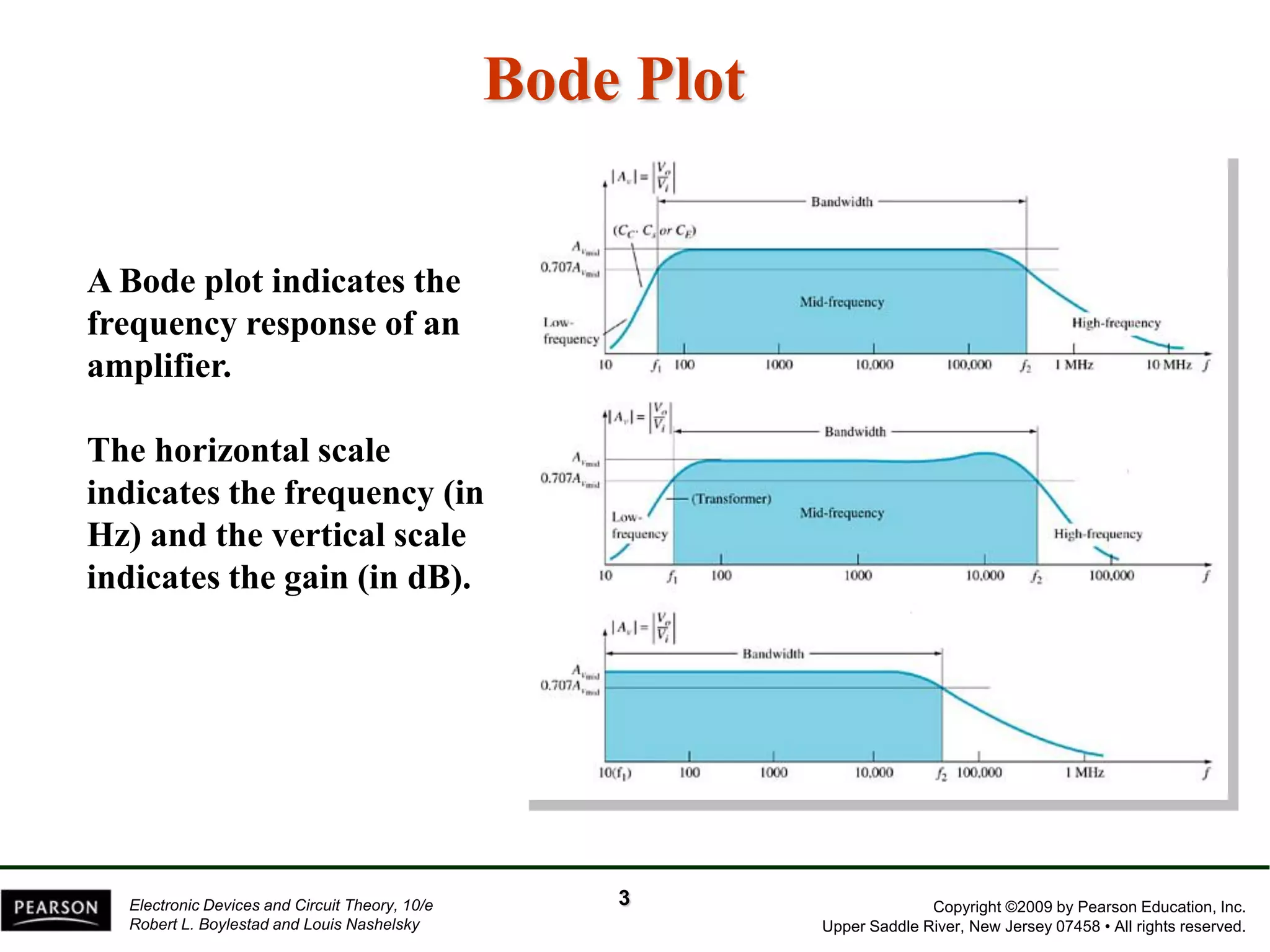
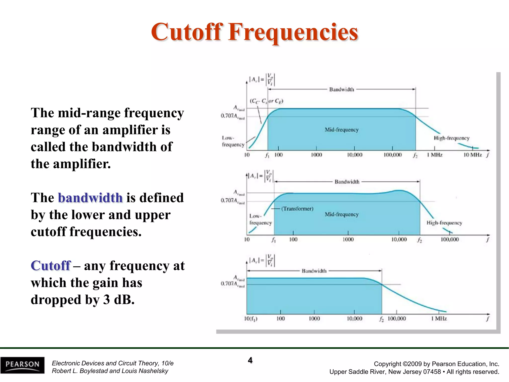
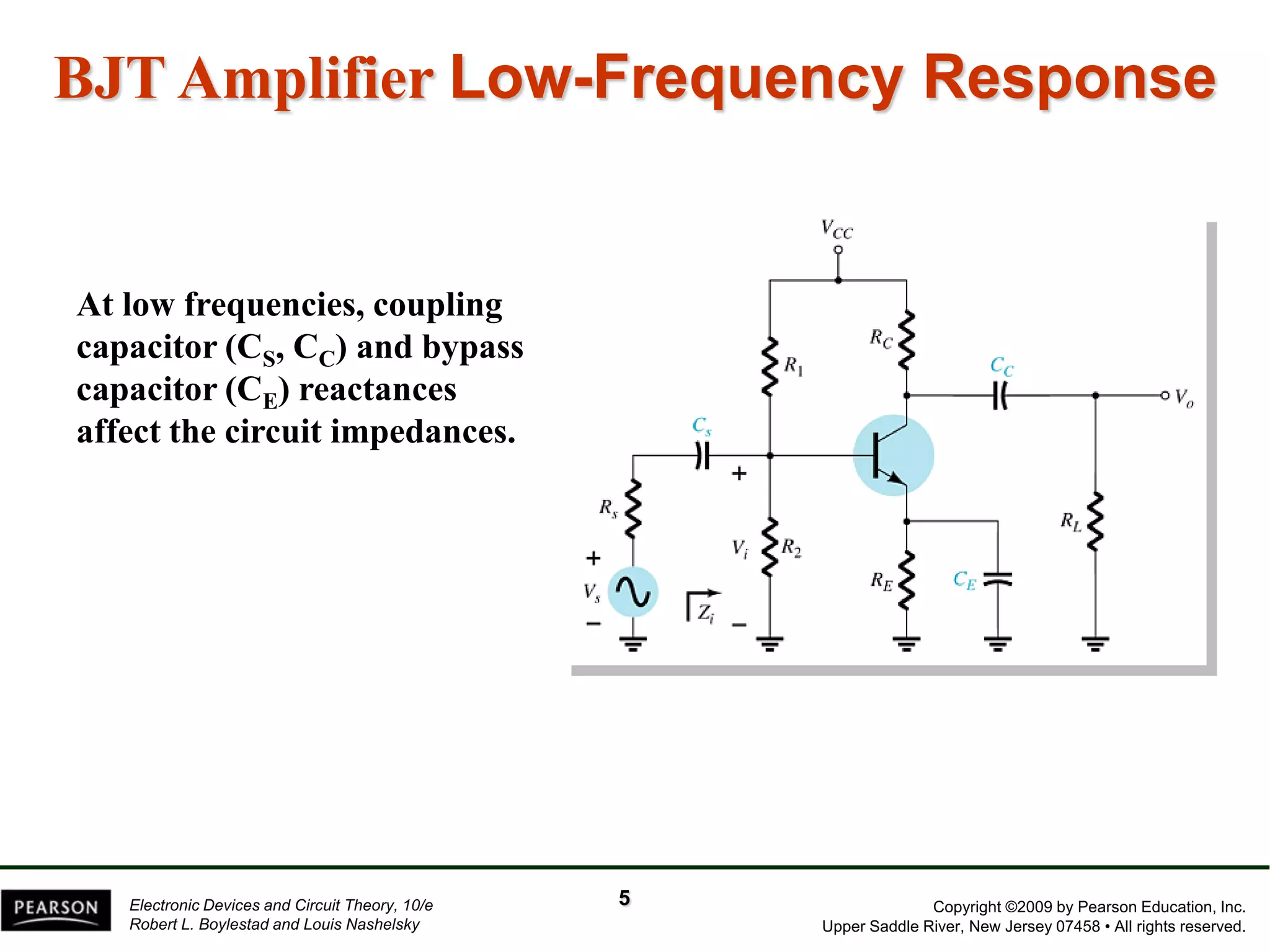
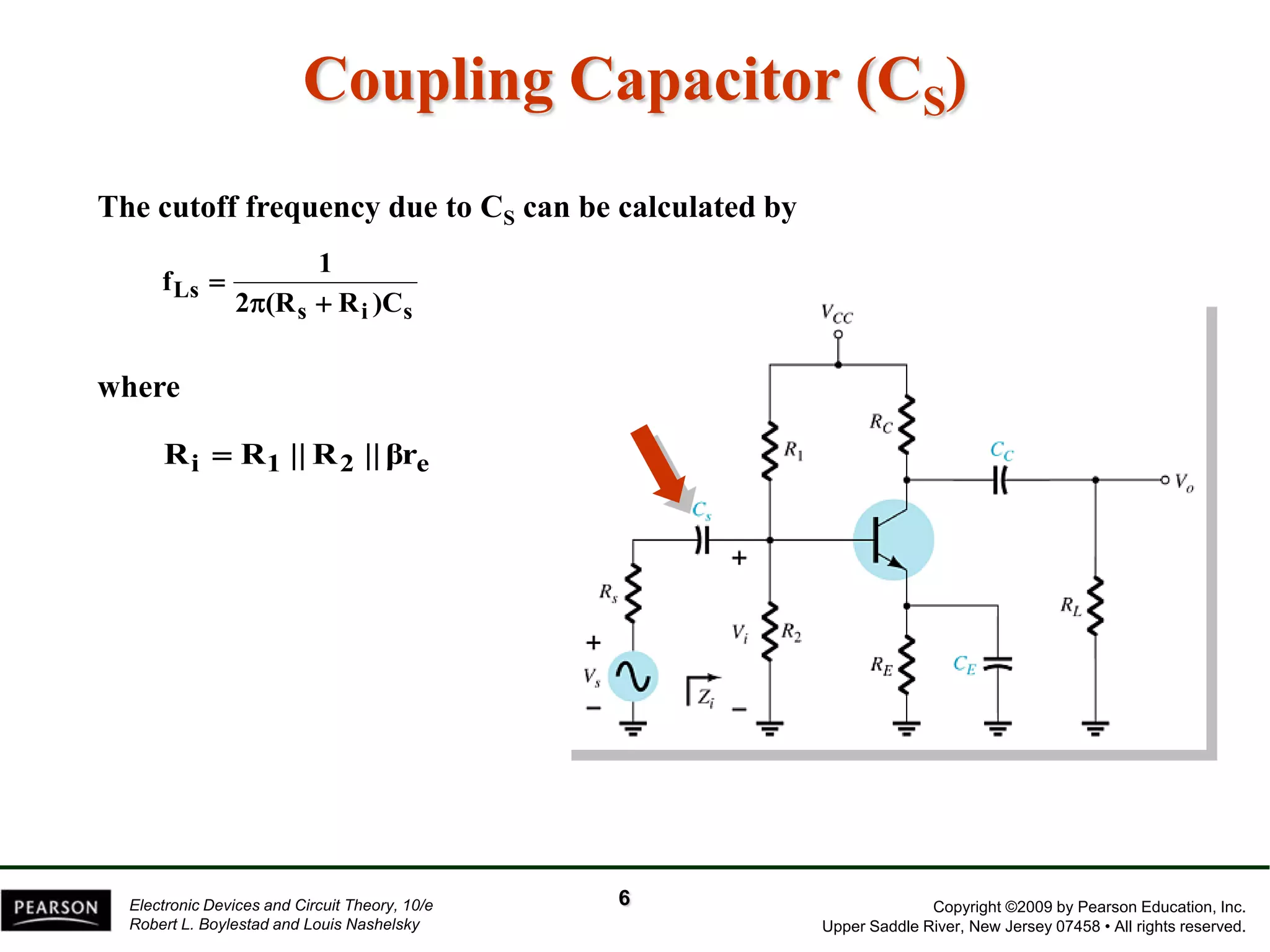
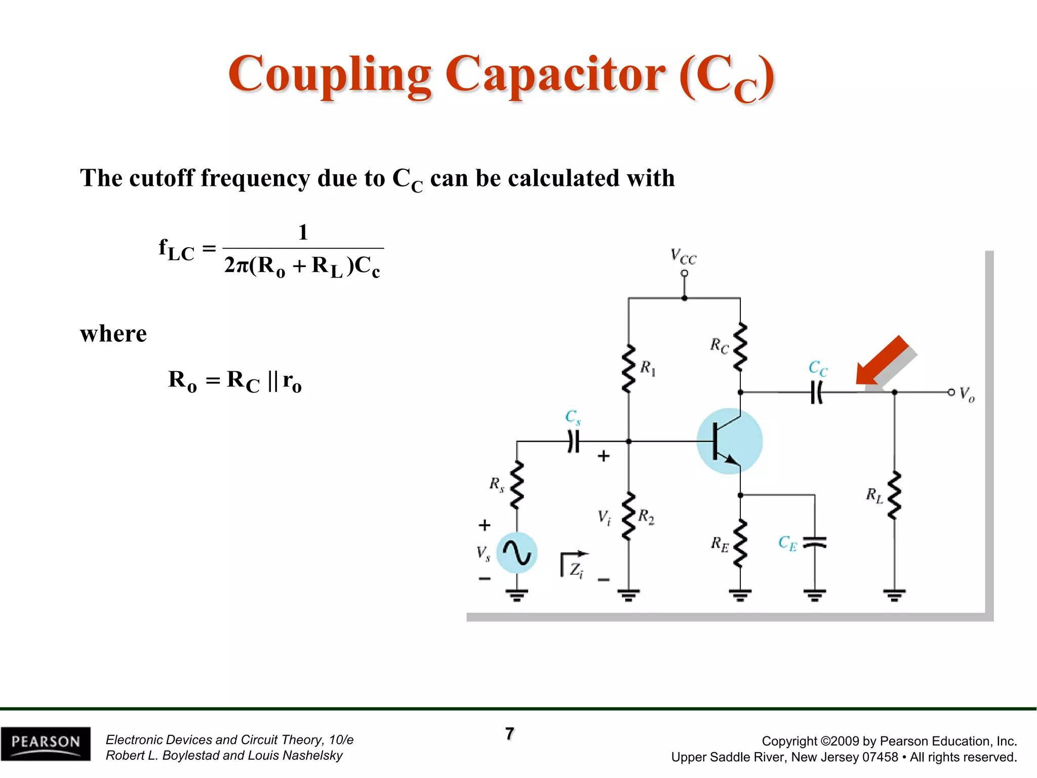
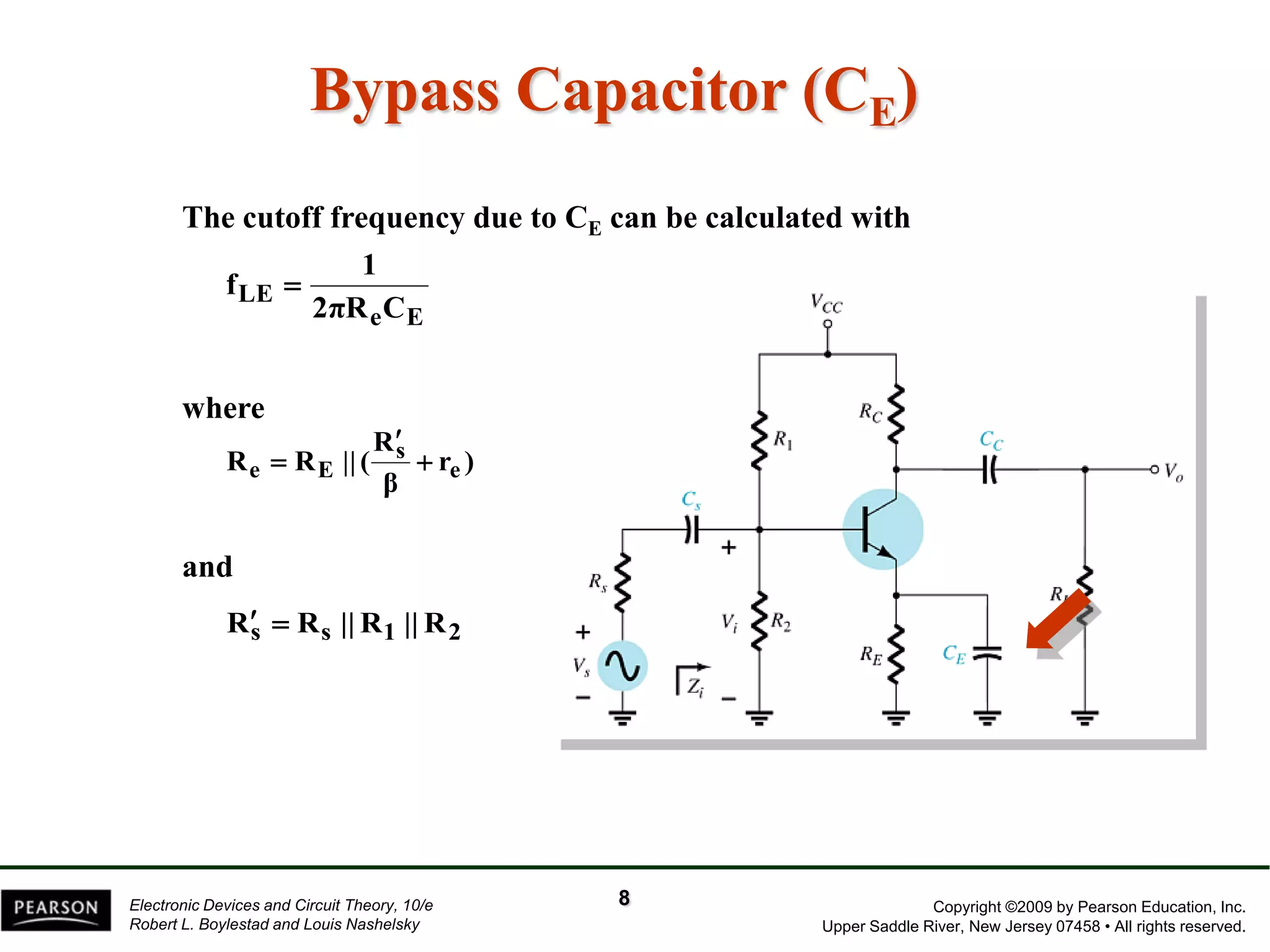
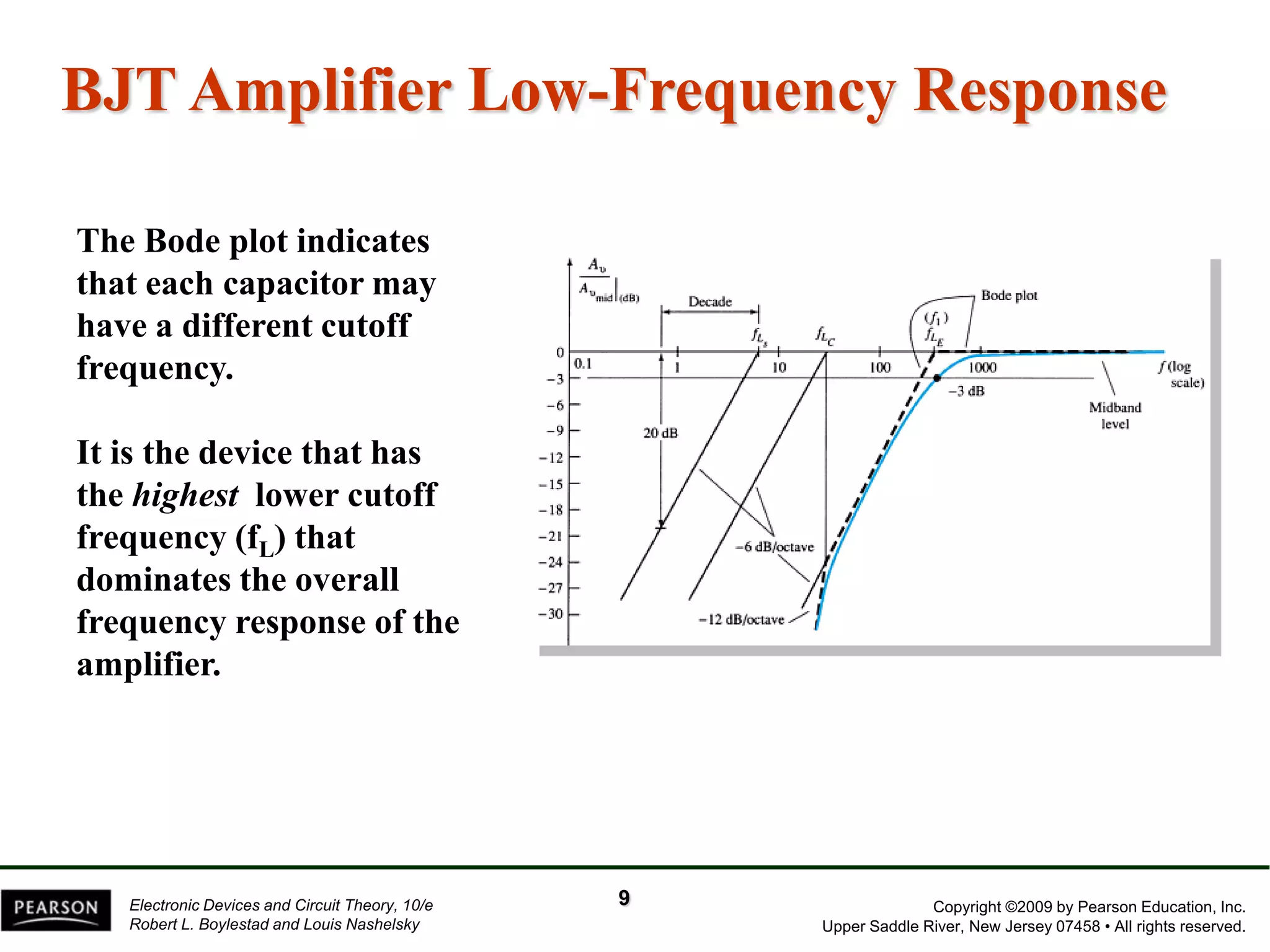
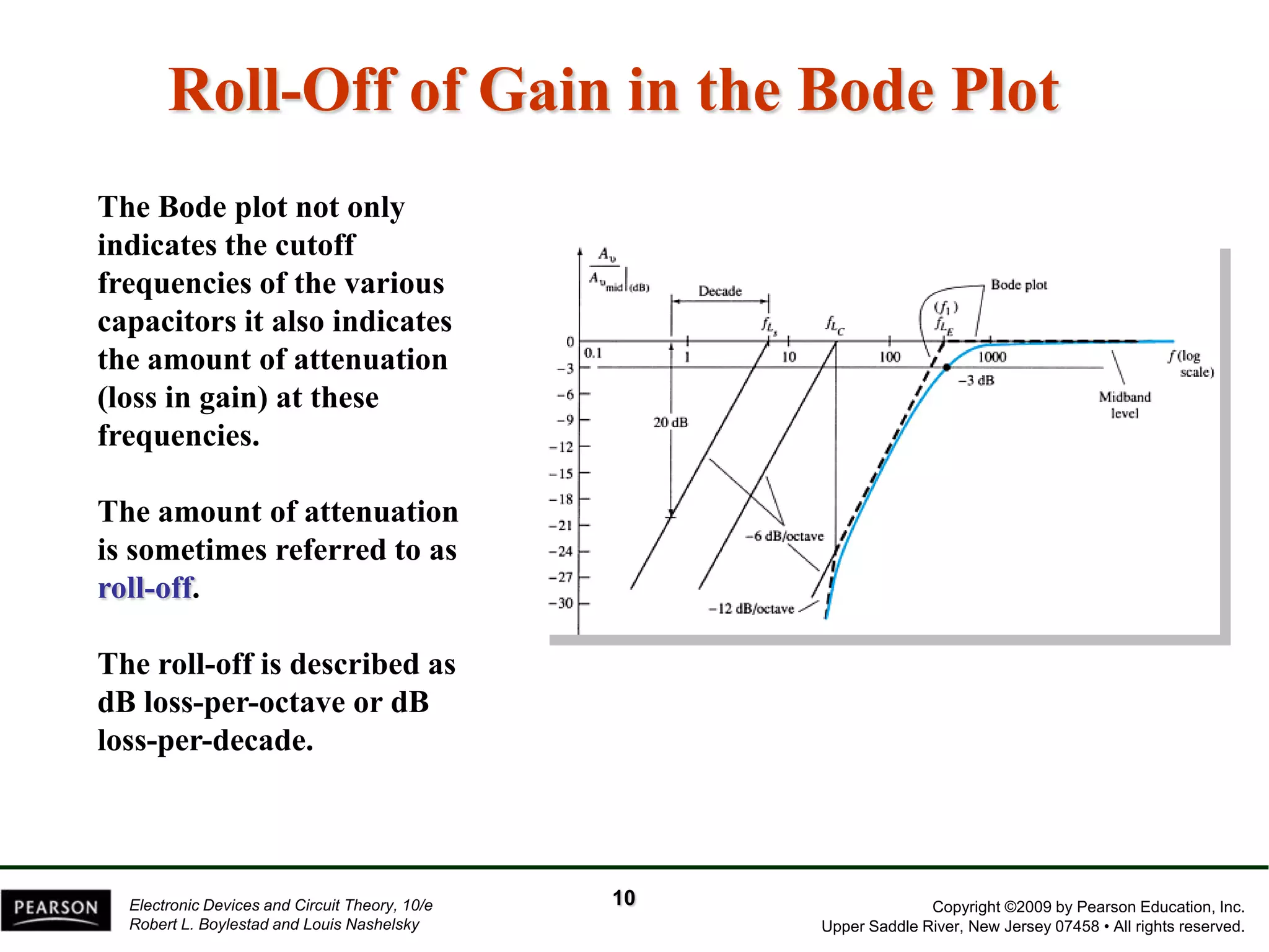
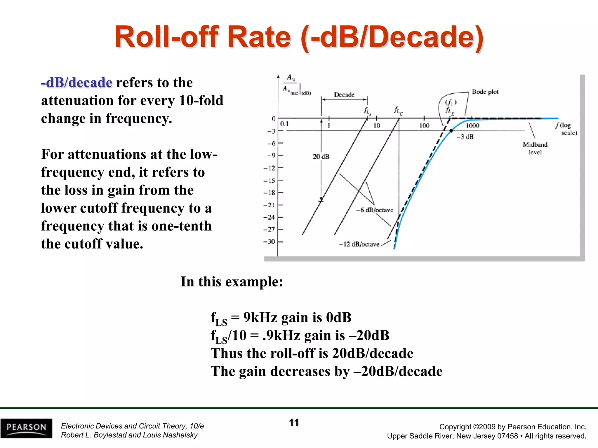
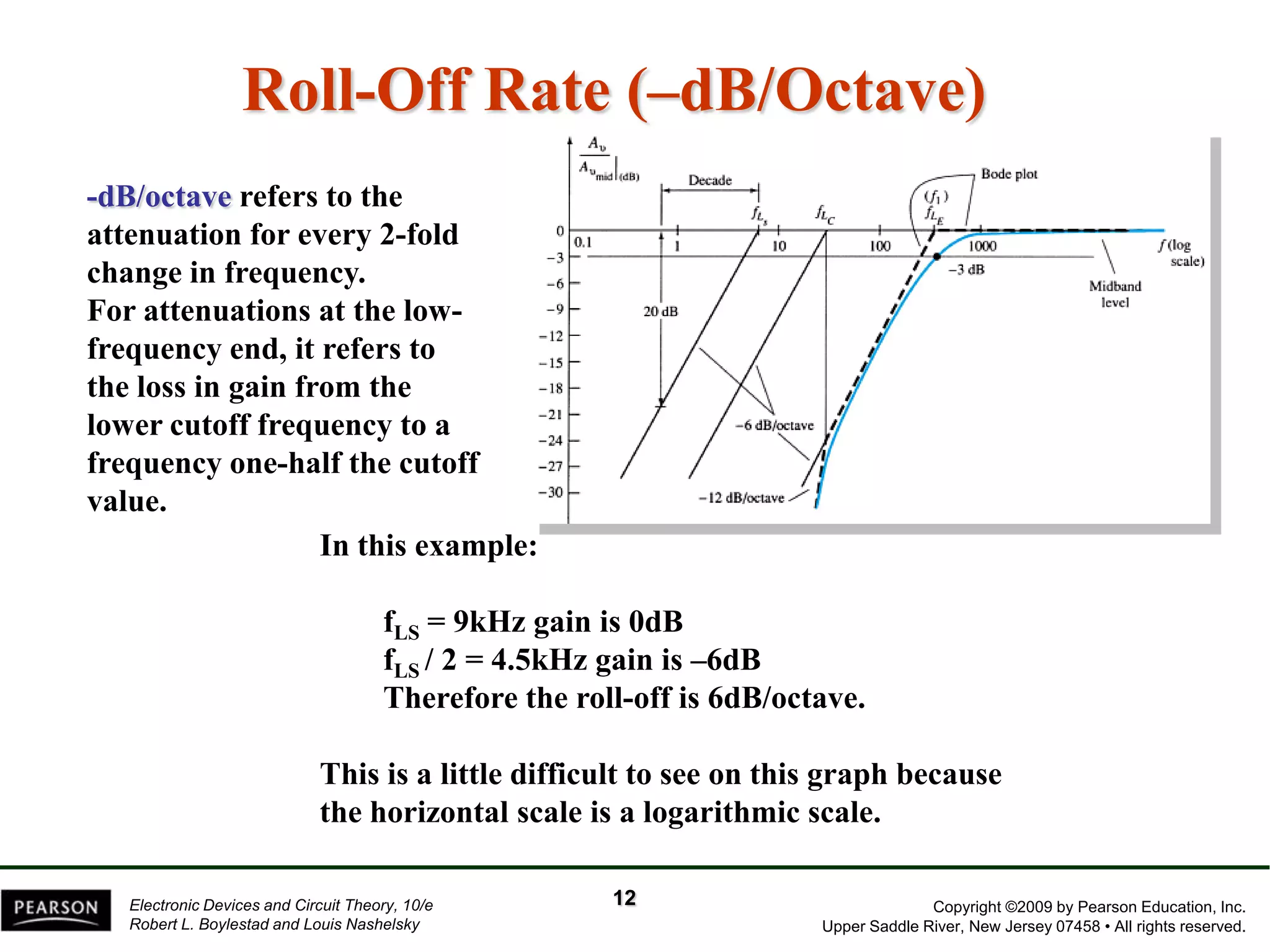
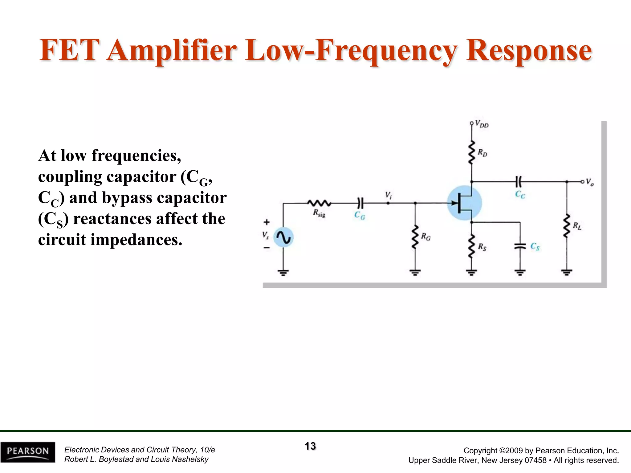
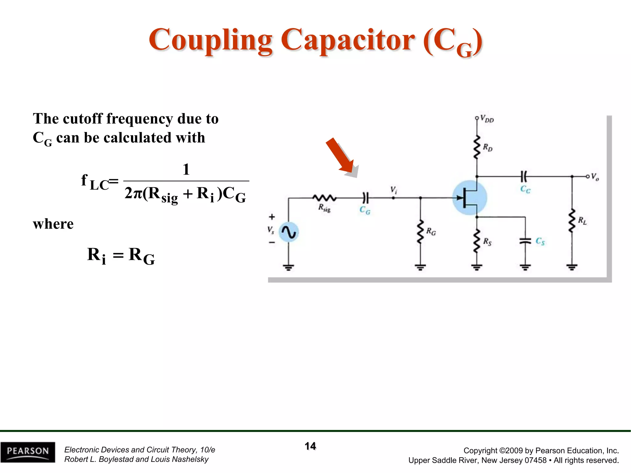
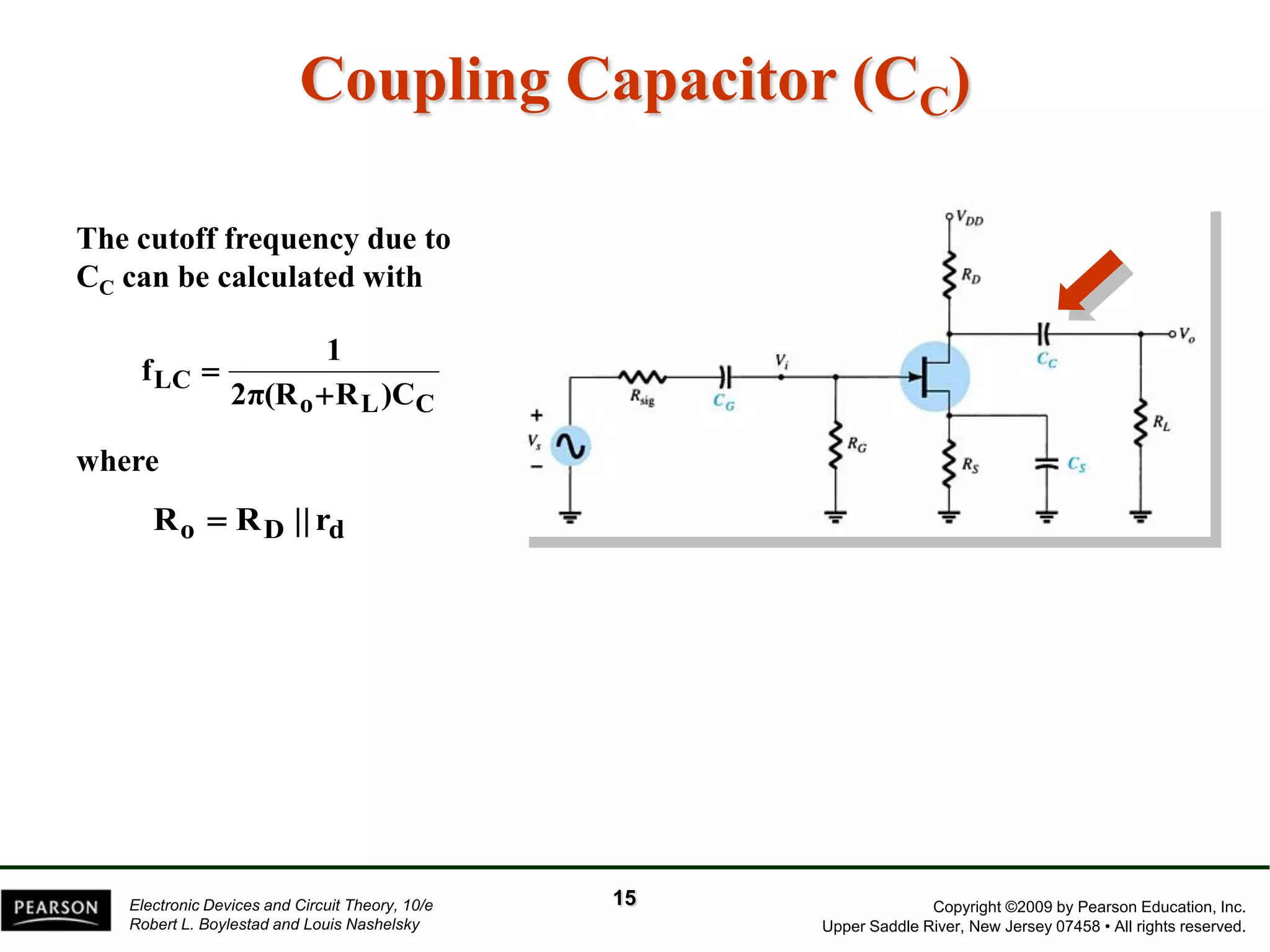
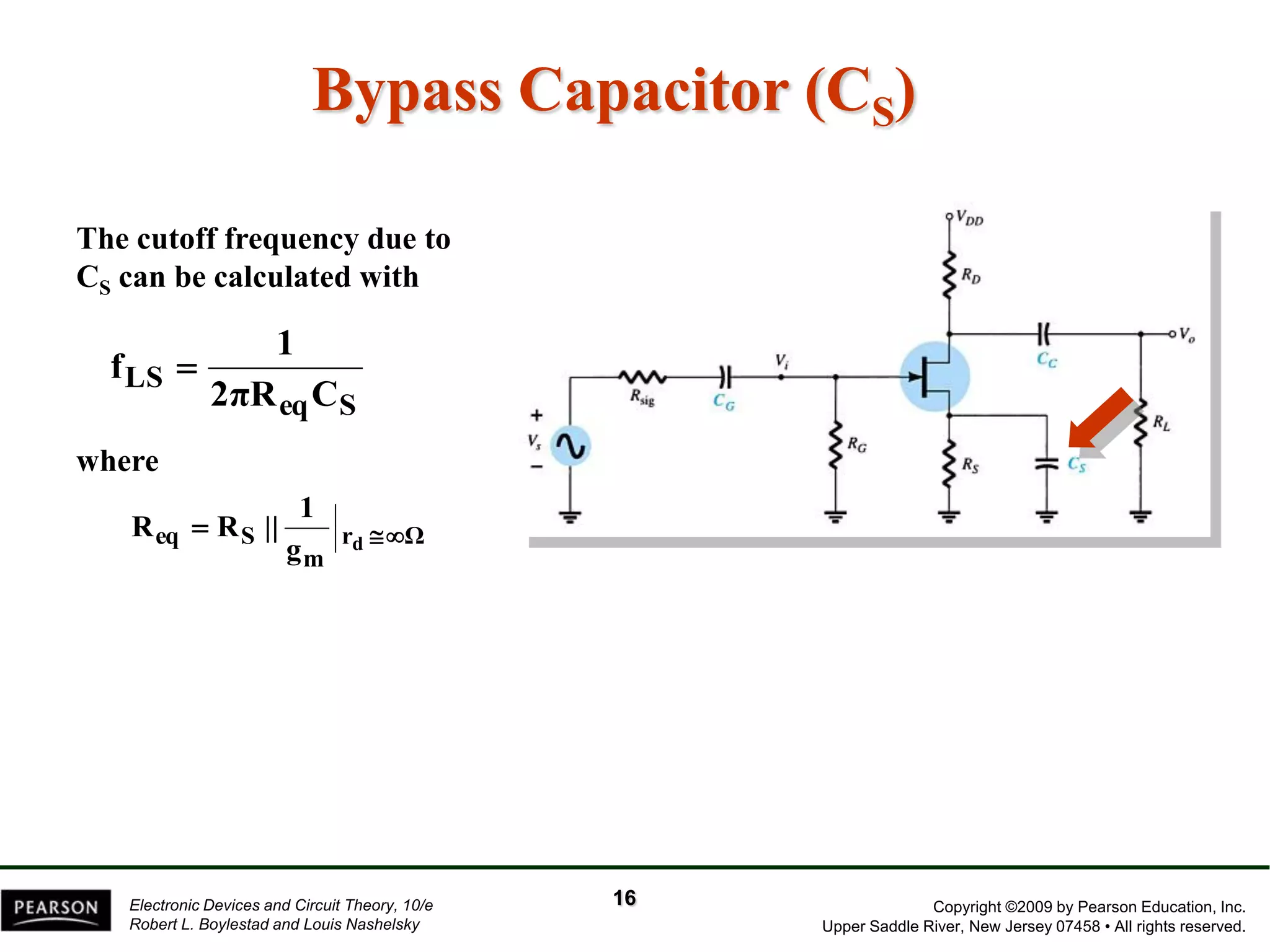
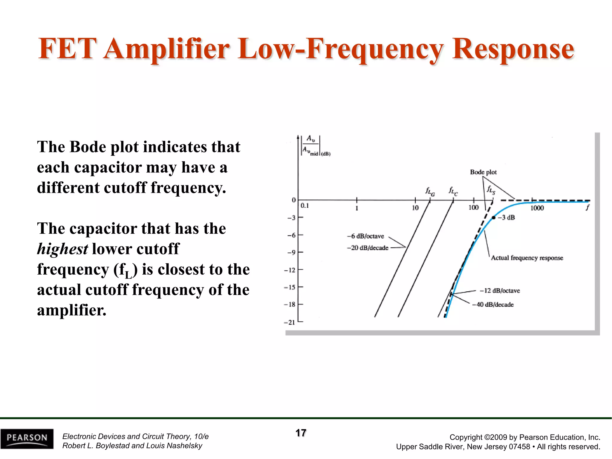
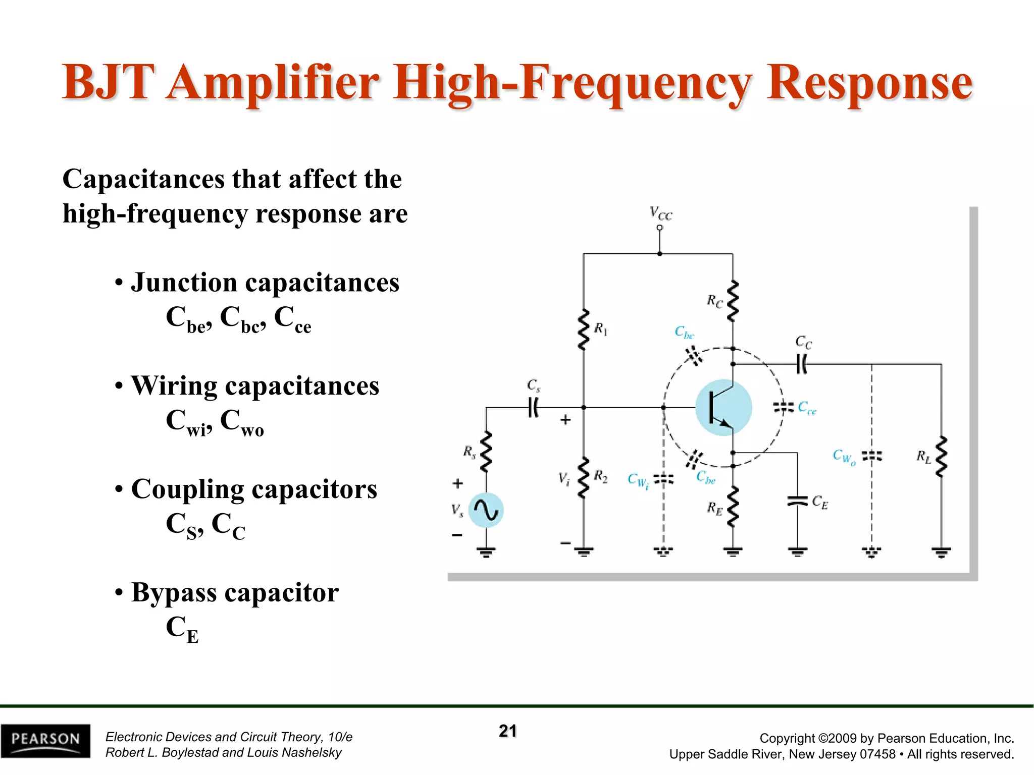
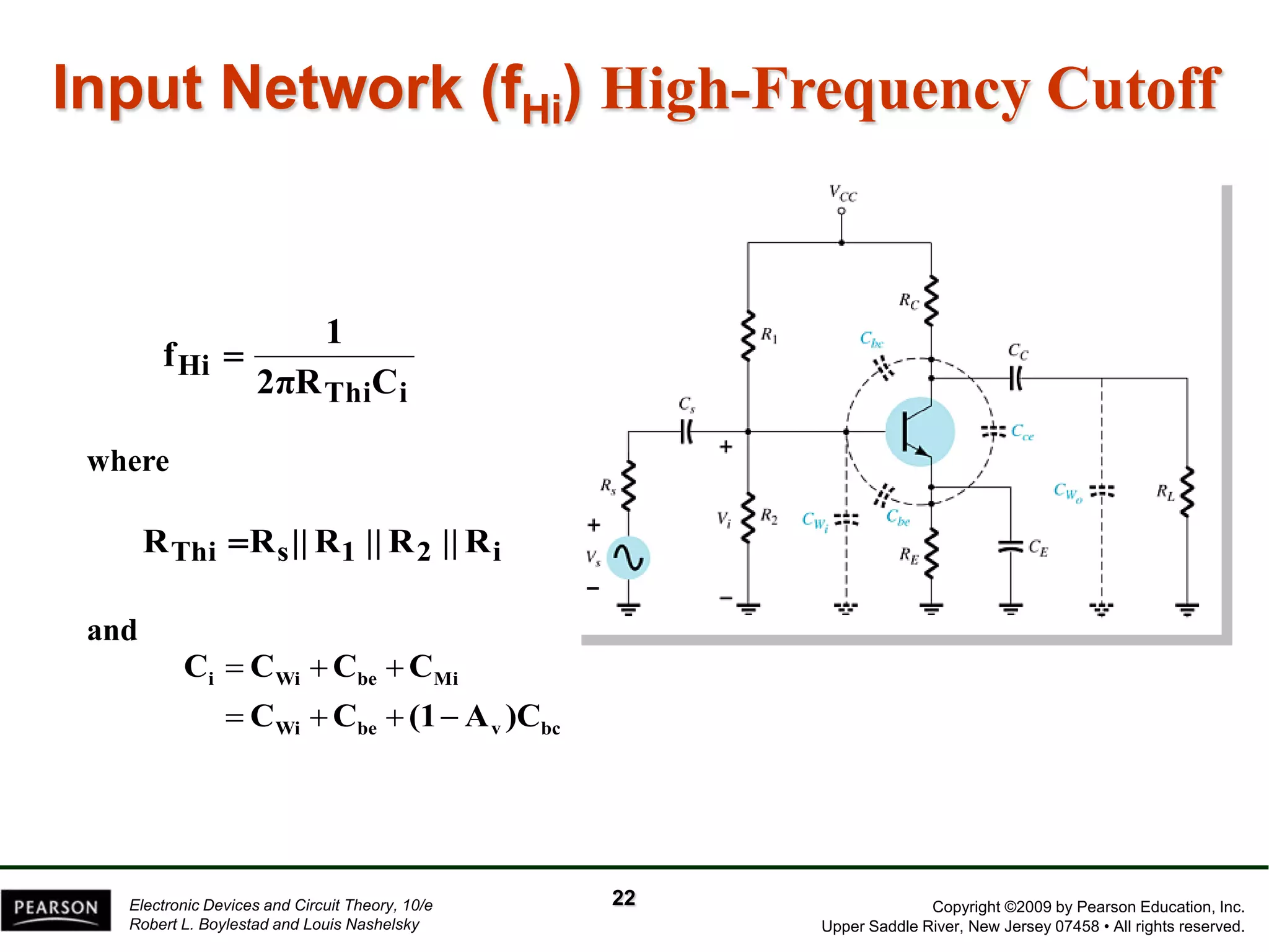
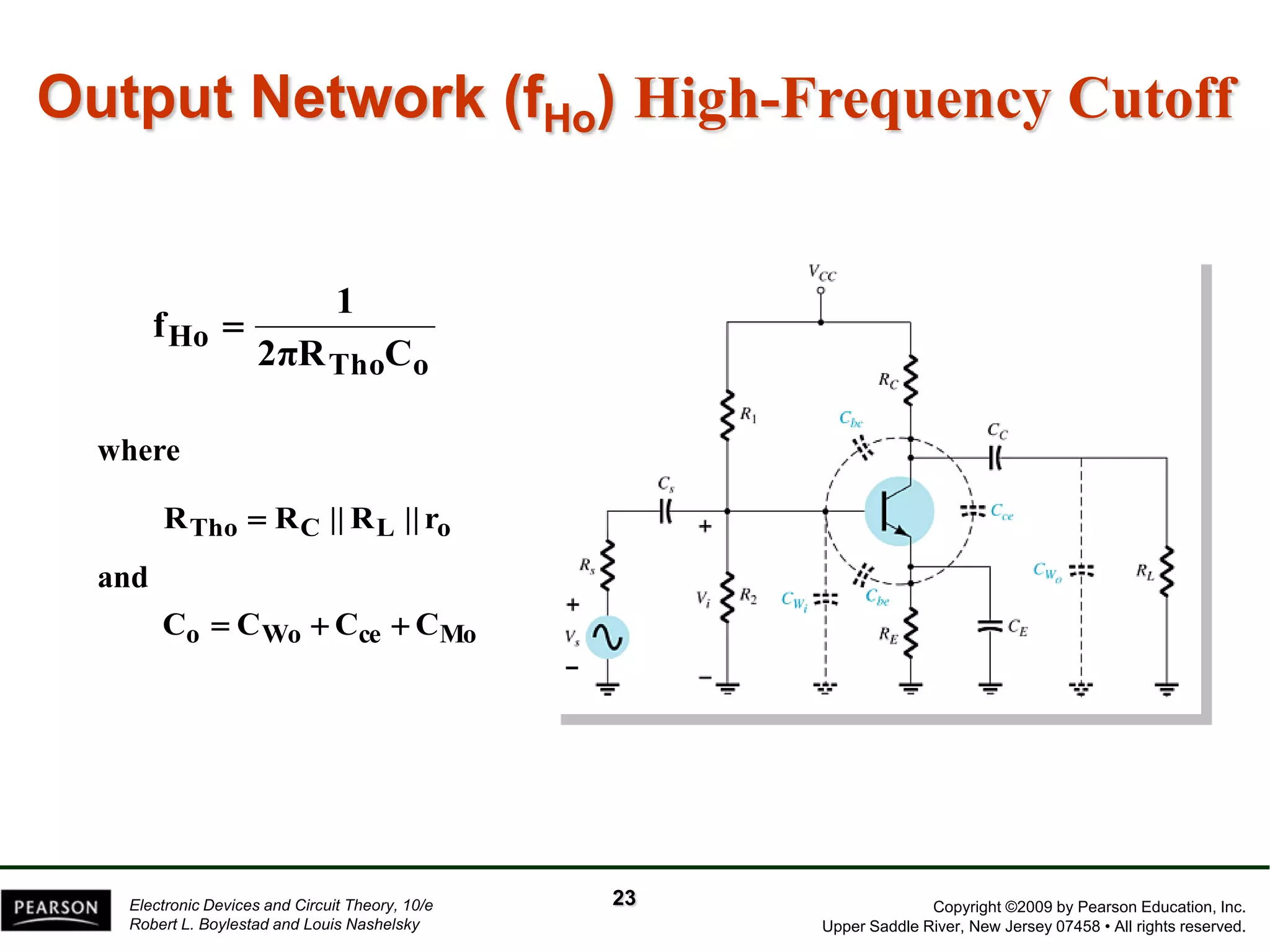
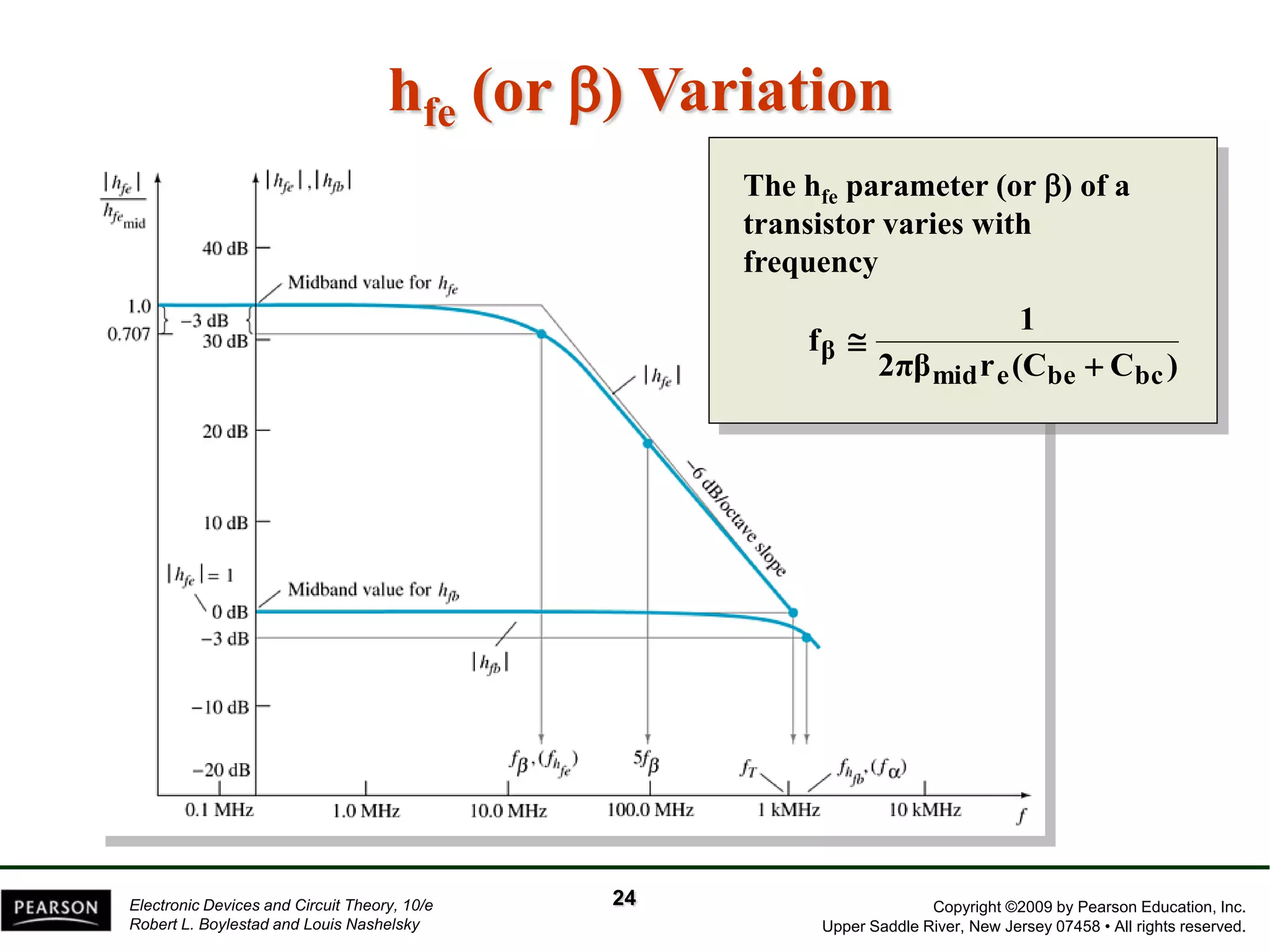
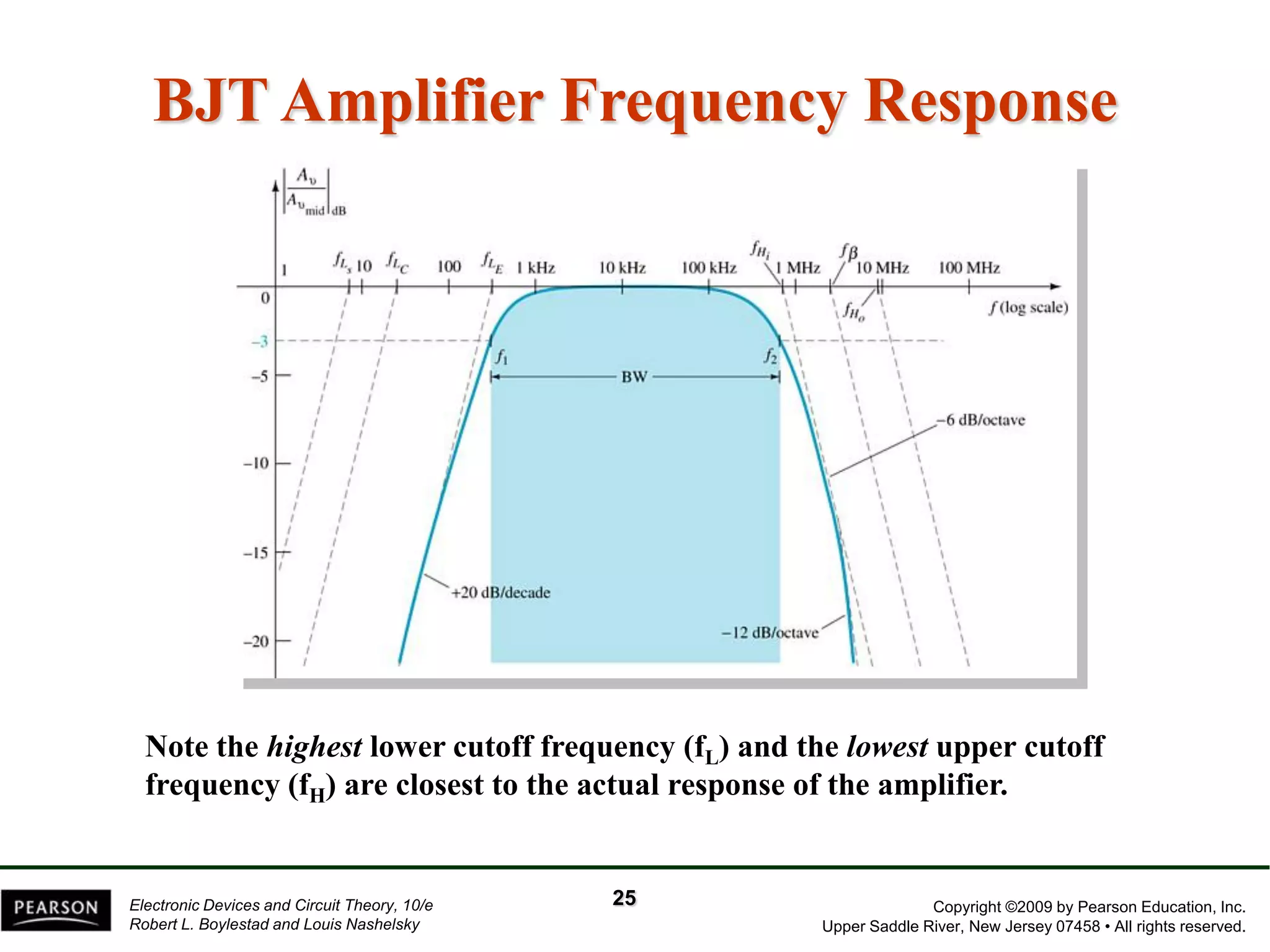
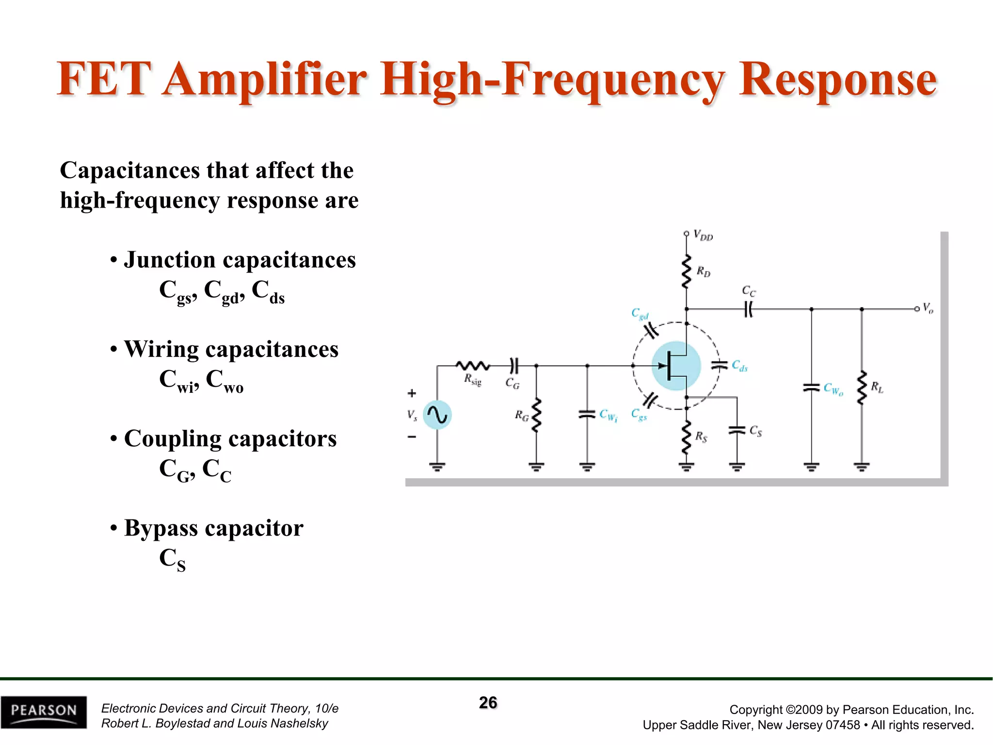
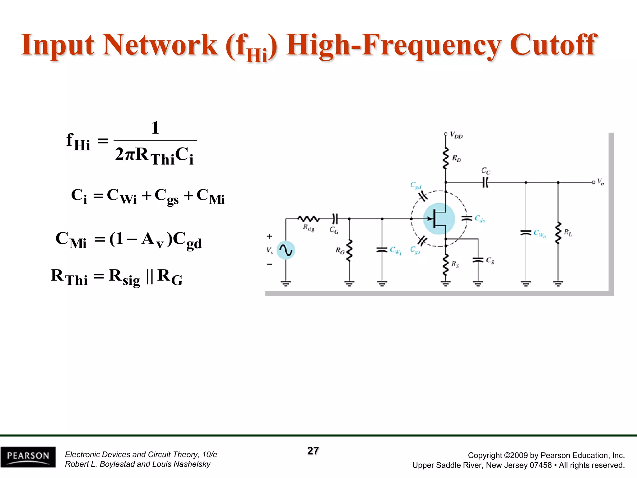
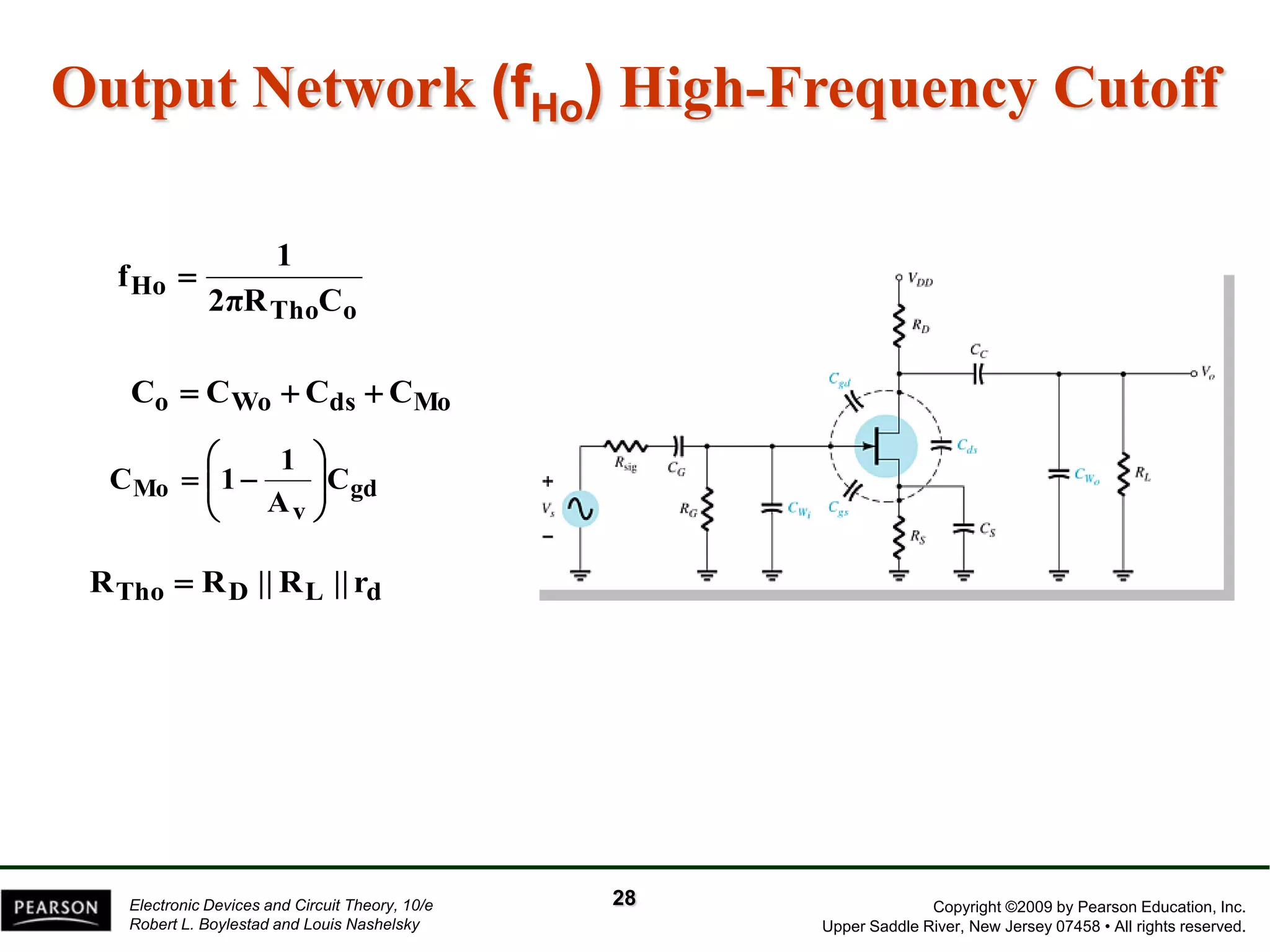

The document discusses the frequency response of BJT and FET amplifiers. It explains that at low frequencies, coupling and bypass capacitors lower the gain, while at high frequencies, stray capacitances associated with the active device lower the gain. The frequency range where an amplifier operates with negligible effects from capacitors is called the mid-range or bandwidth. Bode plots are used to illustrate the cutoff frequencies and roll-off of gain outside this bandwidth. The various factors that determine the low and high frequency cutoffs are analyzed.


![RF Circuit Design - [Ch2-2] Smith Chart](https://cdn.slidesharecdn.com/ss_thumbnails/ch2-2-150613064401-lva1-app6891-thumbnail.jpg?width=640&height=640&fit=bounds)


