The document discusses FET amplifiers, including:
- FETs provide excellent voltage gain, high input impedance, low power consumption, and a good frequency range.
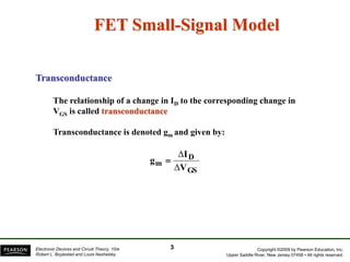
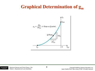
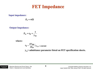
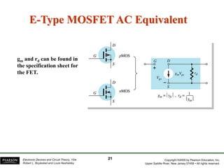
- Transconductance (gm) is the relationship between a change in drain current (ID) to the corresponding change in gate-source voltage (VGS).
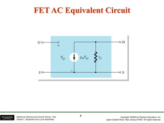
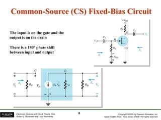
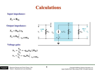
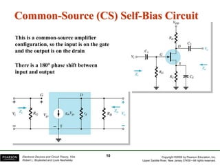
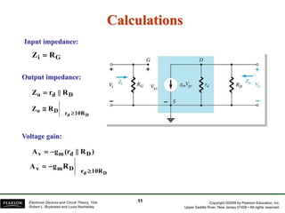
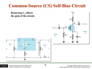
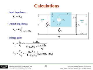
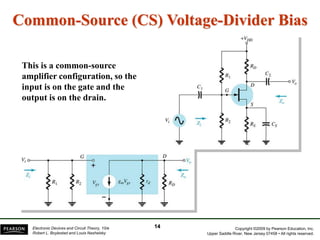
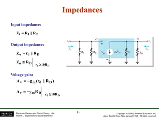
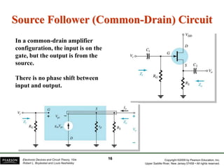
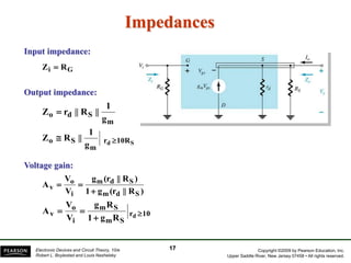
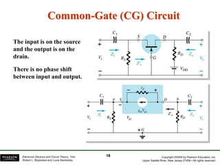
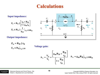
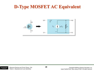
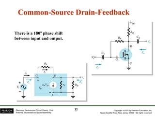
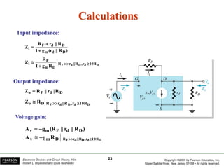
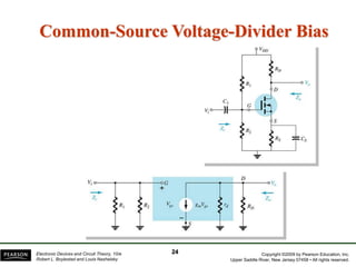
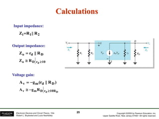
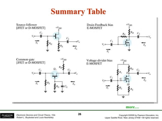
- There are several common FET amplifier configurations - common-source, common-gate, common-drain, and their input/output relationships and calculations for voltage gain, input and output impedances.


![[Deck] What's New in Spark-Iceberg Integration via DSV2.pptx](https://cdn.slidesharecdn.com/ss_thumbnails/deckwhatsnewinspark-icebergintegrationviadsv2-260210005337-25955b12-thumbnail.jpg?width=640&height=640&fit=bounds)
