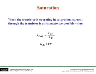
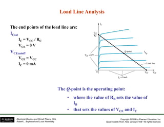
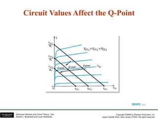
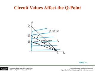
This document summarizes key concepts about biasing BJTs:
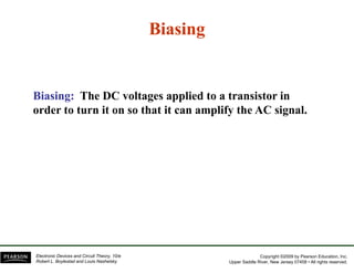
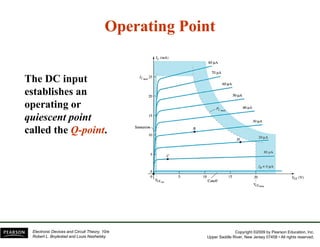
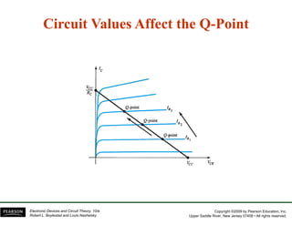
1) Biasing involves applying DC voltages to turn on a transistor so it can amplify an AC signal. This establishes an operating point called the Q-point.
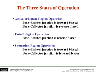
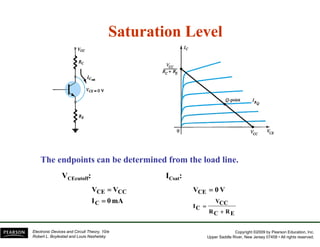
2) There are three regions of transistor operation depending on junction biases: active, cutoff, and saturation.
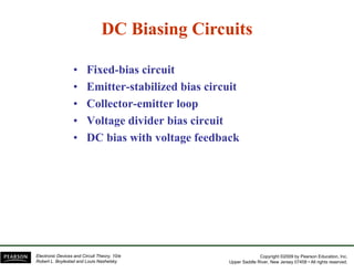
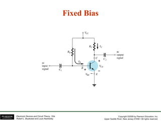
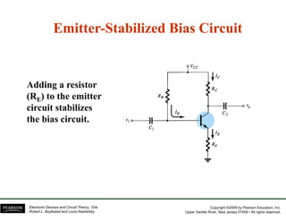
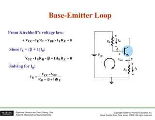
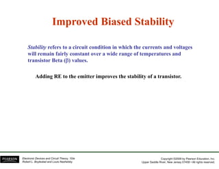
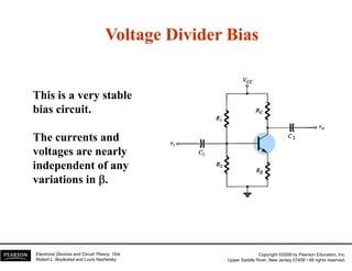
3) Common bias circuits include fixed bias, emitter-stabilized bias, and voltage divider bias. Adding a resistor to the emitter improves stability.


![Bipolar Junction Transistor Biasing [Types]](https://cdn.slidesharecdn.com/ss_thumbnails/ele307module2working-1-251030220651-e41b5c93-thumbnail.jpg?width=640&height=640&fit=bounds)


![Ce drawing[lab]fwddrawing project drawings part two](https://cdn.slidesharecdn.com/ss_thumbnails/cedrawinglabfwddrawingprojectdrawingsparttwo-210425101132-thumbnail.jpg?width=640&height=640&fit=bounds)
![Ce drawing[lab]fwddrawing project drawings part one](https://cdn.slidesharecdn.com/ss_thumbnails/cedrawinglabfwddrawingprojectdrawingspartone-210425101128-thumbnail.jpg?width=640&height=640&fit=bounds)


![[Deck] What's New in Spark-Iceberg Integration via DSV2.pptx](https://cdn.slidesharecdn.com/ss_thumbnails/deckwhatsnewinspark-icebergintegrationviadsv2-260210005337-25955b12-thumbnail.jpg?width=640&height=640&fit=bounds)


