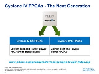
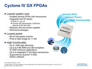
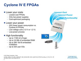
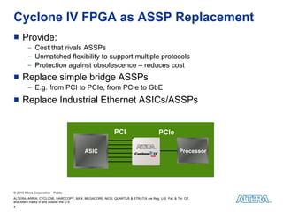
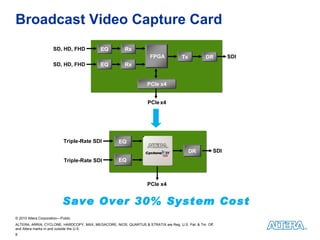
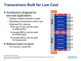
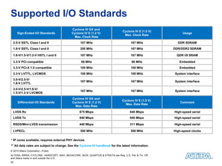
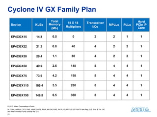
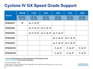
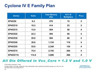
Lowest Cost, Lowest Power, Integrated Transceivers March 2010 Cyclone IV FPGAs
Cyclone IV FPGAs - The Next Generation www.altera.com/products/devices/cyclone-iv/cyiv-index.jsp Cyclone IV GX FPGAs Cyclone IV E FPGAs Lowest cost and lowest power FPGAs with transceivers Lowest cost and lowest  power FPGAs
Cyclone IV GX FPGAs Lowest system cost Smallest density FPGA with transceivers Integrated hard IP blocks PCIe x1, x2, x4 Proven GX transceivers, built from  ground up for low cost Requires only two power supplies Wire-bond packages Lowest power 60-nm low-power process PCIe to GbE bridge for <1.5W High functionality Up to 150K logic elements Up to 6.5 Mb RAM and 360 multipliers  for DSP-intensive applications Up to 8 integrated 3.125-Gbps transceivers Supported by Quartus ®  II Web  Edition software Lowest Cost Lowest Power High Functionality
Cyclone IV E FPGAs Lower your costs  Lowest cost FPGAs Only two power supplies Cost-optimized packaging Lower your power 25% lower power consumption vs. Cyclone III FPGAs Low-voltage core (1.0 V or 1.2 V) Low-power process High functionality Up to 115K LE of logic Up to 3.8 Mb of embedded RAM Up to 266 18x18 embedded multipliers Up to 535 user I/Os Lowest Cost Lowest Power High Functionality
Lowest System Cost Device integration No or lower cost heat sinks Lower layer count PCB Only 2 power supplies Low-cost transceiver I/Os Wire-bond packaging Hard IP uses no FPGA logic $ Lowest Device Costs Lowest BOM Costs
Lower System Costs  Through  Integration DDR PCIe PHY x4 GbE MAC/PHY DAC ADC Save Over 30% in Costs DDR GbE PHY DAC ADC PCIe x4 FPGA GbE x1 BOM Cost Savings Board Cost Savings Cost-reduced, next-generation FPGA Fewer devices through integration Integrated hard IP block Smaller FPGA package Fewer power regulators Reduced thermal needs
Cyclone IV FPGA as ASSP Replacement Provide: Cost that rivals ASSPs Unmatched flexibility to support multiple protocols Protection against obsolescence – reduces cost Replace simple bridge ASSPs  E.g. from PCI to PCIe, from PCIe to GbE Replace Industrial Ethernet ASICs/ASSPs ASIC ASSP 1 PCIe PCI ASIC Processor
Broadcast Video Capture Card EQ EQ Rx Rx FPGA Tx DR PCle x4 PCle x4 SD, HD, FHD SD, HD, FHD SDI Save Over 30% System Cost PCle x4 EQ EQ DR Triple-Rate SDI SDI Triple-Rate SDI
Consumer Video Displays Meet High Video Quality Requirements Quickly and Cost Effectively Tuner Board Tuner ASSP Panel Board TCON 4Kx2K/3D (12b, 240 Hz) V-by-One Tuner Board Tuner ASSP Panel Board ASIC/ FPGA TCON 720p/1080p LVDS
Low-Power Leadership Cyclone III FPGA Cyclone IV E FPGA (1.0 V) Relative Total Power 25% Cyclone III  FPGA + ASSP Cyclone IV GX FPGA Transceiver ASSP + I/O Interface 30% 1.0 1.0
Cyclone IV GX Key Architectural Features MPLL – Multi-purpose phase-locked loop for transceivers Up to 150K LEs Up to 8 Transceivers, up to 3.125 Gbps PCIe Hard IP Block Up to 6.5-Mb Embedded Memory Up to 4 MPLLs  Up to 400-Mbps  External Memory  Interfaces Up to 360 Embedded Multipliers Up to 475 Flexible User I/O Pins Up to 4 PLLs
Transceivers Built for Low Cost Architecture designed for  low-cost applications Support multiple protocols in quad Reconfigure transceivers while in use Optimized PLL sharing Rx and Tx can use the same  or different PLL Unused MPLLs can be used  for FPGA fabric Unused GPLLs can be used  for transceivers Reduce board re-spins Pre-emphasis, equalization XCVR CH 7 XCVR CH 6 MPLL – Tx/Rx MPLL – Tx/Rx XCVR CH 5 XCVR CH 4 XCVR CH 3 XCVR CH 2 MPLL – Tx/Rx MPLL – Tx/Rx XCVR CH 1 XCVR CH 0 GPLL GPLL Quad Quad
Automated transceiver design speeds design entry Supports popular high-speed protocols and IP GUI-Based Transceiver Design Get Your Protocol Set Up Quickly
Simple instantiation and guaranteed timing closure No PCIe licensing fee required Lowest cost entry point for integrated PCIe x1, x2, and x4 Root port and endpoint configurations PCI-SIG compliance Lowest Cost PCIe Solution 30K LE Device EP4CGX15 User Logic (15K LEs) PCIe Hard IP Soft PCIe (15K LEs) User Logic (15K LEs)
Easy-to-Design Transceiver I/Os Feature Benefit PCIe hard IP block No timing closure required Pre-emphasis and equalization Optimize signal integrity without re-spinning PCB General board design guidelines Proven Altera design guidelines Power distribution network (PDN) analyzer Optimize board for each design
Cyclone IV GX Protocol Support 5700 ppm  spread-spectrum  clocking only supported on EP4CGX30F484, EP4CGX50, and EP4CGX75 See the  Cyclone IV handbook   for the latest spec upgrades Protocol Max. Bandwidth (Gbps) QN148, F169, and F324 support* F484, F672, and F896 support IP PCIe Gen1.1 2.5 Yes Yes Included with FPGA GbE 1.25 Yes Yes Altera Basic (proprietary) Up to 2.5 Up to 3.125 N/A CPRI 3.072 Yes Altera XAUI 3.125 Yes Altera Triple-Rate SDI 2.97 Yes Altera Serial RapidIO ® 3.125 Yes Altera V-by-One 3.0 Yes* 3 rd  party DisplayPort  2.7 Yes* 3 rd  party SATA 3.0 Yes* 3 rd  party
Protocol Support in Software Protocol Quartus II Software v9.1 Quartus II Software v9.1 SP1 Quartus II Software v9.1 SP2 Quartus II Software v10.0 PCIe x1, x4     GbE     PCIe x2    Basic    SRIO   XAUI   CPRI  SDI  V-by-One  DisplayPort  SATA 
Memory Optimizations Higher memory-to-logic ratio Packet buffers and caches Buffering for transceiver data Optimized memory-to-multiplier ratio for video and wireless processing applications LEs 9 Kbits Memory (Mb) Cyclone IV E FPGAs Cyclone III FPGAs Cyclone IV GX FPGA M9K 18 36 or 18 36 or M9K Up to 6.5 Mb on-chip memory Cyclone IV GX FPGAs
Automatically Calibrating Memory Interfaces Calibrates for process differences For both FPGA  and  memory Removes timing uncertainties  Monitors voltage and temperature variations  Adjusts resynchronization  phase (PLL output) Does not interrupt operation Supports DDR, DDR2, and  Mobile DDR* memories Minimize Timing Closure Effort External  Memory Memory Controller IP PHY IP Flexibility to use Altera or custom memory controller  Auto-calibrating PHY minimizes effort for reliable timing closure *Mobile DDR support planned for mid-2010 / / / /
Supported I/O Standards * IP cores available, requires external PHY devices ** All data rates are subject to change. See the  Cyclone IV handbook  for the latest information. Sign-Ended I/O Standards Cyclone IV GX and  Cyclone IV E (1.2 V)  Max. Clock Rate Cyclone IV E (1.0 V) Max. Clock Rate Usage 2.5-V SSTL Class I and II 167 MHz 167 MHz DDR SDRAM 1.8-V SSTL Class I and II 200 MHz 167 MHz DDR/DDR2 SDRAM 1.8-V/1.5-V/1.2-V HSTL I and II 167 MHz 167 MHz QDR I/II SRAM 3.3-V PCI compatible 66 MHz 66 MHz Embedded 3.3-V PCI-X 1.0 compatible 100 MHz 100 MHz Embedded 3.3-V LVTTL, LVCMOS 100 MHz 100 MHz System interface 3.0-V/2.5-V/ 1.8-V LVTTL 167 MHz 167 MHz System interface 3.0-V/2.5-V/1.8-V/ 1.5-V/1.2-V LVCMOS 167 MHz 167 MHz System interface Differential I/O Standards Cyclone IV GX and  Cyclone IV E (1.2 V) Max. Data Rate Cyclone IV E (1.0 V)  Max. Data Rate Comment LVDS Rx 875 Mbps 640 Mbps High-speed serial LVDS Tx 840 Mbps 640 Mbps High-speed serial RSDS/Mini-LVDS transmission 440 Mbps 311 Mbps High-speed serial LVPECL 500 MHz 500 MHz High-speed clocks
Increase productivity with easy-to-use Quartus II software SOPC Builder DSP Builder Integrated IP with SOPC Builder Configure transceiver protocols through GUI Online training tools Quartus II software training and demos Interactive tutorials Webcasts Quartus II software manual and handbook Quartus II Software Cyclone IV Support in Quartus II  Web Edition Software v9.1 and Later
Finish Faster   with  Altera Design Tools Tools Benefit Reference designs Get up and running faster with several reference designs IP (protocol packs) Get protocols up quickly (protocol packs for PCIe, GbE, and SRIO) IP portfolio Over 100 pre-built building blocks to jump start your design Development kit Prebuilt, prototyping platform
Cyclone IV GX Family Plan Device KLEs Total Memory (Mb) 18 X 18  Multipliers Transceiver I/Os MPLLs PLLs Hard PCIe IP Core EP4CGX15 14.4 0.5 0 2 2 1 1 EP4CGX22 21.3 0.8 40 4 2 2 1 EP4CGX30 29.4 1.1 80 4 2 2 1 EP4CGX50 49.9 2.5 140 8 4 4 1 EP4CGX75 73.9 4.2 198 8 4 4 1 EP4CGX110 109.4 5.5 280 8 4 4 1 EP4CGX150 149.8 6.5 360 8 4 4 1
Cyclone IV GX Package Plan All packages are wire bond and come in both leaded and RoHS-compliant options     QN148 F169 F324 F484 F672 F896 0.5 mm  11 x 11 1.0 mm  14 x 14 1.0 mm  19 x 19 1.0 mm  23 x 23 1.0 mm  27 x 27 1.0 mm  31 x 31 Device I/Os XCVRs I/Os XVCRs I/Os XCVRs I/Os XCVRs I/Os XCVRs I/Os XCVRs EP4CGX15 72 2 72 2                 EP4CGX22     72 2 150 4             EP4CGX30     72 2 150 4   290 4          EP4CGX50             290 4 310 8     EP4CGX75             290 4 310 8     EP4CGX110             270 4 393 8 475 8 EP4CGX150             270 4 393 8 475 8
Cyclone IV GX Speed Grade Support *-7 and -I7 speed grades are under evaluation for this package. See the  Cyclone IV handbook   for the latest information.   Device QN148 F169 F324 F484 F672 F896 0.5 mm  11 x 11 1.0 mm  14 x 14 1.0 mm  19 x 19 1.0 mm  23 x 23 1.0 mm  27 x 27 1.0 mm  31 x 31 EP4CGX15 -8* -6, -7, -8, -I7 EP4CGX22 -6, -7, -8, -I7 -6, -7, -8, -I7 EP4CGX30 -6, -7, -8, -I7 -6, -7, -8, -I7 -6, -7, -8, -I7 EP4CGX50 -6, -7, -8, -I7  -6, -7, -8, -I7 EP4CGX75 -6, -7, -8, -I7 -6, -7, -8, -I7 EP4CGX110 -7, -8, -I7 -7, -8, -I7 -7, -8, -I7 EP4CGX150 -7, -8, -I7 -7, -8, -I7 -7, -8, -I7
Cyclone IV E Family Plan All Die Offered in Vcc_Core = 1.2 V and 1.0 V Device KLEs Total Memory (Kb) 18 X 18  Multipliers PLLs EP4CE6 6.2 270 15 2 EP4CE10 10.3 414 23 2 EP4CE15 15.4 504 56 4 EP4CE22 22.3 594 66 4 EP4CE30 28.8 594 66 4 EP4CE40 39.6 1,134 116 4 EP4CE55 55.8 2,340 154 4 EP4CE75 75.4 2,745 200 4 EP4CE115 114.4 3,888 266 4
Cyclone IV E Package Plan All packages are wire bond and come in both leaded and RoHS-compliant options   E144 F256 F484 F780 Device 22 x 22 mm 0.5 mm 17 x 17 mm 1.0 mm 23 x 23 mm 1.0 mm 29 x 29 mm 1.0 mm EP4EC6 91 179 EP4CE10 91 179 EP4CE15 81 165 343 EP4CE22 79 153 N/A EP4CE30 328 532 EP4CE40 328 532 EP4CE55 324 374 EP4CE75 292 426 EP4CE115 280 528
Cyclone IV E Speed Grade Support Note: I = industrial grade (Tj = -40 ° C to 100 ° C); A = automotive grade (Tj = -40 ° C to 125 ° C), L = 1.0-V Vcc core variant   E144 F256 F484 F780 Device 22 x 22 mm 0.5 mm 17 x 17 mm 1.0 mm 23 x 23 mm 1.0 mm 29 x 29 mm 1.0 mm EP4C6E -6, -7, -8, -I7, -A7 -8L, -9L, -I8L -6, -7, -8, -I7, -A7 -8L, -9L, -I8L EP4C10E Same as above Same as above EP4C15E -6, -7, -8, -I7 -8L, -9L, -I8L Same as above -6, -7, -8, -I7, -A7 -8L, -9L, -I8L EP4C22E -6, -7, -8, -I7, -A7 -8L, -9L, -I8L Same as above EP4C30E Same as above -6, -7, -8, -I7 -8L, -9L, -I8L EP4C40E Same as above Same as above EP4C55E -6, -7, -8, -I7 -8L, -9L, -I8L Same as above EP4C75E Same as above Same as above EP4C115E -7, -8, -I7 -8L, -9L, -I8L -7, -8, -I7 -8L, -9L, -I8L
Features to Meet the Needs of High-Volume Applications 2K – 20K logic elements (LEs) 295 Kb embedded RAM DDR support Nios embedded processor 5K – 70K LEs 1.1 Mb embedded RAM  150 18 x 18 multipliers for DSP DDR2 support Nios II embedded processor 50% lower power  5K – 200K LEs 8 Mb embedded RAM 396 18 x 18 multipliers for DSP Higher performance DDR2 support Nios II embedded processor Complete security solution Integrated transceivers Up to 30% lower power Only 2 power supplies Integrated PCIe hard IP 6K – 150K LEs 6.5 Mb of embedded RAM Up to 360 multipliers Nios II embedded processor 2002 2004 2007 2009
Cyclone IV GX Device Rollout Schedule Notes: Consult your local sales representative for rollout dates for the other commercial and industrial speed grades. Product Line Availability (-C8 Speed Grades) Software Compilation Support EP4CGX15 March Quartus II software v9.1 SP1 EP4CGX150 July EP4CGX110 August EP4CGX22 September EP4CGX30 up to  F324 package September EP4CGX30 (F484 only) December EP4CGX75 December EP4CGX50 December
Cyclone IV E Device Rollout Schedule Notes: Rollout for –C6 and -8L speed grades will be 2 weeks after dates shown above. Rollout for –i7 and -i8L speed grades will be 3 weeks after dates shown above. Product Line Availability (-C8 and -9L Speed Grades) Software Support EP4CE115 March 31 (1.0 V) Quartus II software v9.1 SP1 (1.2 V) Quartus II software v9.1 SP2 EP4CE55 April 5 EP4CE6 April 12 EP4CE10 April 12 EP4CE15 April 26 EP4CE75 April 26 EP4CE30 April 30 EP4CE40 April 30 EP4CE22 May 10
Cyclone IV Development  Kits Altera Cyclone IV GX Transceiver Starter Kit (see below) Cyclone IV GX150 dev kit (3Q 2010) Partners EBV DB4CGX15 dev kit with add-on boards Terasic EP4CE115 university kit Terasic Cyclone IV E industrial networking kit Cost:  $395.00 P/N:  DK-START-4CGX15N Pre-order now…call distributors

Altera Cyclone IV FPGA Customer Presentation

  • 1.
    Lowest Cost, LowestPower, Integrated Transceivers March 2010 Cyclone IV FPGAs
  • 2.
    Cyclone IV FPGAs- The Next Generation www.altera.com/products/devices/cyclone-iv/cyiv-index.jsp Cyclone IV GX FPGAs Cyclone IV E FPGAs Lowest cost and lowest power FPGAs with transceivers Lowest cost and lowest power FPGAs
  • 3.
    Cyclone IV GXFPGAs Lowest system cost Smallest density FPGA with transceivers Integrated hard IP blocks PCIe x1, x2, x4 Proven GX transceivers, built from ground up for low cost Requires only two power supplies Wire-bond packages Lowest power 60-nm low-power process PCIe to GbE bridge for <1.5W High functionality Up to 150K logic elements Up to 6.5 Mb RAM and 360 multipliers for DSP-intensive applications Up to 8 integrated 3.125-Gbps transceivers Supported by Quartus ® II Web Edition software Lowest Cost Lowest Power High Functionality
  • 4.
    Cyclone IV EFPGAs Lower your costs Lowest cost FPGAs Only two power supplies Cost-optimized packaging Lower your power 25% lower power consumption vs. Cyclone III FPGAs Low-voltage core (1.0 V or 1.2 V) Low-power process High functionality Up to 115K LE of logic Up to 3.8 Mb of embedded RAM Up to 266 18x18 embedded multipliers Up to 535 user I/Os Lowest Cost Lowest Power High Functionality
  • 5.
    Lowest System CostDevice integration No or lower cost heat sinks Lower layer count PCB Only 2 power supplies Low-cost transceiver I/Os Wire-bond packaging Hard IP uses no FPGA logic $ Lowest Device Costs Lowest BOM Costs
  • 6.
    Lower System Costs Through Integration DDR PCIe PHY x4 GbE MAC/PHY DAC ADC Save Over 30% in Costs DDR GbE PHY DAC ADC PCIe x4 FPGA GbE x1 BOM Cost Savings Board Cost Savings Cost-reduced, next-generation FPGA Fewer devices through integration Integrated hard IP block Smaller FPGA package Fewer power regulators Reduced thermal needs
  • 7.
    Cyclone IV FPGAas ASSP Replacement Provide: Cost that rivals ASSPs Unmatched flexibility to support multiple protocols Protection against obsolescence – reduces cost Replace simple bridge ASSPs E.g. from PCI to PCIe, from PCIe to GbE Replace Industrial Ethernet ASICs/ASSPs ASIC ASSP 1 PCIe PCI ASIC Processor
  • 8.
    Broadcast Video CaptureCard EQ EQ Rx Rx FPGA Tx DR PCle x4 PCle x4 SD, HD, FHD SD, HD, FHD SDI Save Over 30% System Cost PCle x4 EQ EQ DR Triple-Rate SDI SDI Triple-Rate SDI
  • 9.
    Consumer Video DisplaysMeet High Video Quality Requirements Quickly and Cost Effectively Tuner Board Tuner ASSP Panel Board TCON 4Kx2K/3D (12b, 240 Hz) V-by-One Tuner Board Tuner ASSP Panel Board ASIC/ FPGA TCON 720p/1080p LVDS
  • 10.
    Low-Power Leadership CycloneIII FPGA Cyclone IV E FPGA (1.0 V) Relative Total Power 25% Cyclone III FPGA + ASSP Cyclone IV GX FPGA Transceiver ASSP + I/O Interface 30% 1.0 1.0
  • 11.
    Cyclone IV GXKey Architectural Features MPLL – Multi-purpose phase-locked loop for transceivers Up to 150K LEs Up to 8 Transceivers, up to 3.125 Gbps PCIe Hard IP Block Up to 6.5-Mb Embedded Memory Up to 4 MPLLs Up to 400-Mbps External Memory Interfaces Up to 360 Embedded Multipliers Up to 475 Flexible User I/O Pins Up to 4 PLLs
  • 12.
    Transceivers Built forLow Cost Architecture designed for low-cost applications Support multiple protocols in quad Reconfigure transceivers while in use Optimized PLL sharing Rx and Tx can use the same or different PLL Unused MPLLs can be used for FPGA fabric Unused GPLLs can be used for transceivers Reduce board re-spins Pre-emphasis, equalization XCVR CH 7 XCVR CH 6 MPLL – Tx/Rx MPLL – Tx/Rx XCVR CH 5 XCVR CH 4 XCVR CH 3 XCVR CH 2 MPLL – Tx/Rx MPLL – Tx/Rx XCVR CH 1 XCVR CH 0 GPLL GPLL Quad Quad
  • 13.
    Automated transceiver designspeeds design entry Supports popular high-speed protocols and IP GUI-Based Transceiver Design Get Your Protocol Set Up Quickly
  • 14.
    Simple instantiation andguaranteed timing closure No PCIe licensing fee required Lowest cost entry point for integrated PCIe x1, x2, and x4 Root port and endpoint configurations PCI-SIG compliance Lowest Cost PCIe Solution 30K LE Device EP4CGX15 User Logic (15K LEs) PCIe Hard IP Soft PCIe (15K LEs) User Logic (15K LEs)
  • 15.
    Easy-to-Design Transceiver I/OsFeature Benefit PCIe hard IP block No timing closure required Pre-emphasis and equalization Optimize signal integrity without re-spinning PCB General board design guidelines Proven Altera design guidelines Power distribution network (PDN) analyzer Optimize board for each design
  • 16.
    Cyclone IV GXProtocol Support 5700 ppm spread-spectrum clocking only supported on EP4CGX30F484, EP4CGX50, and EP4CGX75 See the Cyclone IV handbook for the latest spec upgrades Protocol Max. Bandwidth (Gbps) QN148, F169, and F324 support* F484, F672, and F896 support IP PCIe Gen1.1 2.5 Yes Yes Included with FPGA GbE 1.25 Yes Yes Altera Basic (proprietary) Up to 2.5 Up to 3.125 N/A CPRI 3.072 Yes Altera XAUI 3.125 Yes Altera Triple-Rate SDI 2.97 Yes Altera Serial RapidIO ® 3.125 Yes Altera V-by-One 3.0 Yes* 3 rd party DisplayPort 2.7 Yes* 3 rd party SATA 3.0 Yes* 3 rd party
  • 17.
    Protocol Support inSoftware Protocol Quartus II Software v9.1 Quartus II Software v9.1 SP1 Quartus II Software v9.1 SP2 Quartus II Software v10.0 PCIe x1, x4     GbE     PCIe x2    Basic    SRIO   XAUI   CPRI  SDI  V-by-One  DisplayPort  SATA 
  • 18.
    Memory Optimizations Highermemory-to-logic ratio Packet buffers and caches Buffering for transceiver data Optimized memory-to-multiplier ratio for video and wireless processing applications LEs 9 Kbits Memory (Mb) Cyclone IV E FPGAs Cyclone III FPGAs Cyclone IV GX FPGA M9K 18 36 or 18 36 or M9K Up to 6.5 Mb on-chip memory Cyclone IV GX FPGAs
  • 19.
    Automatically Calibrating MemoryInterfaces Calibrates for process differences For both FPGA and memory Removes timing uncertainties Monitors voltage and temperature variations Adjusts resynchronization phase (PLL output) Does not interrupt operation Supports DDR, DDR2, and Mobile DDR* memories Minimize Timing Closure Effort External Memory Memory Controller IP PHY IP Flexibility to use Altera or custom memory controller Auto-calibrating PHY minimizes effort for reliable timing closure *Mobile DDR support planned for mid-2010 / / / /
  • 20.
    Supported I/O Standards* IP cores available, requires external PHY devices ** All data rates are subject to change. See the Cyclone IV handbook for the latest information. Sign-Ended I/O Standards Cyclone IV GX and Cyclone IV E (1.2 V) Max. Clock Rate Cyclone IV E (1.0 V) Max. Clock Rate Usage 2.5-V SSTL Class I and II 167 MHz 167 MHz DDR SDRAM 1.8-V SSTL Class I and II 200 MHz 167 MHz DDR/DDR2 SDRAM 1.8-V/1.5-V/1.2-V HSTL I and II 167 MHz 167 MHz QDR I/II SRAM 3.3-V PCI compatible 66 MHz 66 MHz Embedded 3.3-V PCI-X 1.0 compatible 100 MHz 100 MHz Embedded 3.3-V LVTTL, LVCMOS 100 MHz 100 MHz System interface 3.0-V/2.5-V/ 1.8-V LVTTL 167 MHz 167 MHz System interface 3.0-V/2.5-V/1.8-V/ 1.5-V/1.2-V LVCMOS 167 MHz 167 MHz System interface Differential I/O Standards Cyclone IV GX and Cyclone IV E (1.2 V) Max. Data Rate Cyclone IV E (1.0 V) Max. Data Rate Comment LVDS Rx 875 Mbps 640 Mbps High-speed serial LVDS Tx 840 Mbps 640 Mbps High-speed serial RSDS/Mini-LVDS transmission 440 Mbps 311 Mbps High-speed serial LVPECL 500 MHz 500 MHz High-speed clocks
  • 21.
    Increase productivity witheasy-to-use Quartus II software SOPC Builder DSP Builder Integrated IP with SOPC Builder Configure transceiver protocols through GUI Online training tools Quartus II software training and demos Interactive tutorials Webcasts Quartus II software manual and handbook Quartus II Software Cyclone IV Support in Quartus II Web Edition Software v9.1 and Later
  • 22.
    Finish Faster with Altera Design Tools Tools Benefit Reference designs Get up and running faster with several reference designs IP (protocol packs) Get protocols up quickly (protocol packs for PCIe, GbE, and SRIO) IP portfolio Over 100 pre-built building blocks to jump start your design Development kit Prebuilt, prototyping platform
  • 23.
    Cyclone IV GXFamily Plan Device KLEs Total Memory (Mb) 18 X 18 Multipliers Transceiver I/Os MPLLs PLLs Hard PCIe IP Core EP4CGX15 14.4 0.5 0 2 2 1 1 EP4CGX22 21.3 0.8 40 4 2 2 1 EP4CGX30 29.4 1.1 80 4 2 2 1 EP4CGX50 49.9 2.5 140 8 4 4 1 EP4CGX75 73.9 4.2 198 8 4 4 1 EP4CGX110 109.4 5.5 280 8 4 4 1 EP4CGX150 149.8 6.5 360 8 4 4 1
  • 24.
    Cyclone IV GXPackage Plan All packages are wire bond and come in both leaded and RoHS-compliant options     QN148 F169 F324 F484 F672 F896 0.5 mm 11 x 11 1.0 mm 14 x 14 1.0 mm 19 x 19 1.0 mm 23 x 23 1.0 mm 27 x 27 1.0 mm 31 x 31 Device I/Os XCVRs I/Os XVCRs I/Os XCVRs I/Os XCVRs I/Os XCVRs I/Os XCVRs EP4CGX15 72 2 72 2                 EP4CGX22     72 2 150 4             EP4CGX30     72 2 150 4   290 4          EP4CGX50             290 4 310 8     EP4CGX75             290 4 310 8     EP4CGX110             270 4 393 8 475 8 EP4CGX150             270 4 393 8 475 8
  • 25.
    Cyclone IV GXSpeed Grade Support *-7 and -I7 speed grades are under evaluation for this package. See the Cyclone IV handbook for the latest information.   Device QN148 F169 F324 F484 F672 F896 0.5 mm 11 x 11 1.0 mm 14 x 14 1.0 mm 19 x 19 1.0 mm 23 x 23 1.0 mm 27 x 27 1.0 mm 31 x 31 EP4CGX15 -8* -6, -7, -8, -I7 EP4CGX22 -6, -7, -8, -I7 -6, -7, -8, -I7 EP4CGX30 -6, -7, -8, -I7 -6, -7, -8, -I7 -6, -7, -8, -I7 EP4CGX50 -6, -7, -8, -I7 -6, -7, -8, -I7 EP4CGX75 -6, -7, -8, -I7 -6, -7, -8, -I7 EP4CGX110 -7, -8, -I7 -7, -8, -I7 -7, -8, -I7 EP4CGX150 -7, -8, -I7 -7, -8, -I7 -7, -8, -I7
  • 26.
    Cyclone IV EFamily Plan All Die Offered in Vcc_Core = 1.2 V and 1.0 V Device KLEs Total Memory (Kb) 18 X 18 Multipliers PLLs EP4CE6 6.2 270 15 2 EP4CE10 10.3 414 23 2 EP4CE15 15.4 504 56 4 EP4CE22 22.3 594 66 4 EP4CE30 28.8 594 66 4 EP4CE40 39.6 1,134 116 4 EP4CE55 55.8 2,340 154 4 EP4CE75 75.4 2,745 200 4 EP4CE115 114.4 3,888 266 4
  • 27.
    Cyclone IV EPackage Plan All packages are wire bond and come in both leaded and RoHS-compliant options   E144 F256 F484 F780 Device 22 x 22 mm 0.5 mm 17 x 17 mm 1.0 mm 23 x 23 mm 1.0 mm 29 x 29 mm 1.0 mm EP4EC6 91 179 EP4CE10 91 179 EP4CE15 81 165 343 EP4CE22 79 153 N/A EP4CE30 328 532 EP4CE40 328 532 EP4CE55 324 374 EP4CE75 292 426 EP4CE115 280 528
  • 28.
    Cyclone IV ESpeed Grade Support Note: I = industrial grade (Tj = -40 ° C to 100 ° C); A = automotive grade (Tj = -40 ° C to 125 ° C), L = 1.0-V Vcc core variant   E144 F256 F484 F780 Device 22 x 22 mm 0.5 mm 17 x 17 mm 1.0 mm 23 x 23 mm 1.0 mm 29 x 29 mm 1.0 mm EP4C6E -6, -7, -8, -I7, -A7 -8L, -9L, -I8L -6, -7, -8, -I7, -A7 -8L, -9L, -I8L EP4C10E Same as above Same as above EP4C15E -6, -7, -8, -I7 -8L, -9L, -I8L Same as above -6, -7, -8, -I7, -A7 -8L, -9L, -I8L EP4C22E -6, -7, -8, -I7, -A7 -8L, -9L, -I8L Same as above EP4C30E Same as above -6, -7, -8, -I7 -8L, -9L, -I8L EP4C40E Same as above Same as above EP4C55E -6, -7, -8, -I7 -8L, -9L, -I8L Same as above EP4C75E Same as above Same as above EP4C115E -7, -8, -I7 -8L, -9L, -I8L -7, -8, -I7 -8L, -9L, -I8L
  • 29.
    Features to Meetthe Needs of High-Volume Applications 2K – 20K logic elements (LEs) 295 Kb embedded RAM DDR support Nios embedded processor 5K – 70K LEs 1.1 Mb embedded RAM 150 18 x 18 multipliers for DSP DDR2 support Nios II embedded processor 50% lower power 5K – 200K LEs 8 Mb embedded RAM 396 18 x 18 multipliers for DSP Higher performance DDR2 support Nios II embedded processor Complete security solution Integrated transceivers Up to 30% lower power Only 2 power supplies Integrated PCIe hard IP 6K – 150K LEs 6.5 Mb of embedded RAM Up to 360 multipliers Nios II embedded processor 2002 2004 2007 2009
  • 30.
    Cyclone IV GXDevice Rollout Schedule Notes: Consult your local sales representative for rollout dates for the other commercial and industrial speed grades. Product Line Availability (-C8 Speed Grades) Software Compilation Support EP4CGX15 March Quartus II software v9.1 SP1 EP4CGX150 July EP4CGX110 August EP4CGX22 September EP4CGX30 up to F324 package September EP4CGX30 (F484 only) December EP4CGX75 December EP4CGX50 December
  • 31.
    Cyclone IV EDevice Rollout Schedule Notes: Rollout for –C6 and -8L speed grades will be 2 weeks after dates shown above. Rollout for –i7 and -i8L speed grades will be 3 weeks after dates shown above. Product Line Availability (-C8 and -9L Speed Grades) Software Support EP4CE115 March 31 (1.0 V) Quartus II software v9.1 SP1 (1.2 V) Quartus II software v9.1 SP2 EP4CE55 April 5 EP4CE6 April 12 EP4CE10 April 12 EP4CE15 April 26 EP4CE75 April 26 EP4CE30 April 30 EP4CE40 April 30 EP4CE22 May 10
  • 32.
    Cyclone IV Development Kits Altera Cyclone IV GX Transceiver Starter Kit (see below) Cyclone IV GX150 dev kit (3Q 2010) Partners EBV DB4CGX15 dev kit with add-on boards Terasic EP4CE115 university kit Terasic Cyclone IV E industrial networking kit Cost: $395.00 P/N: DK-START-4CGX15N Pre-order now…call distributors