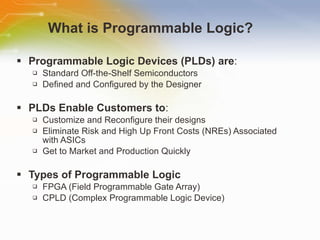
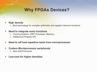
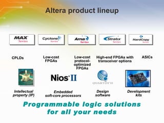
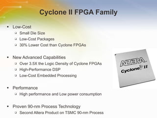
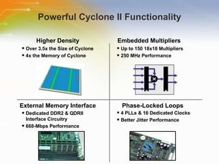
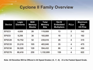
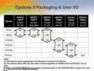
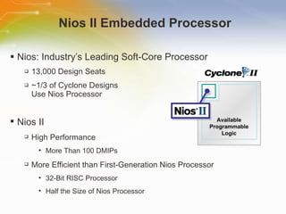
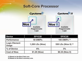
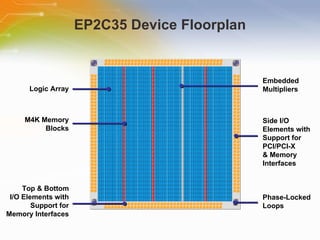
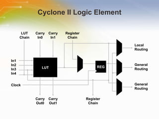
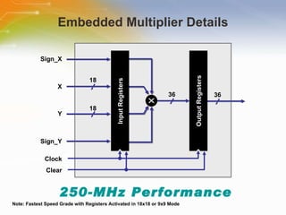
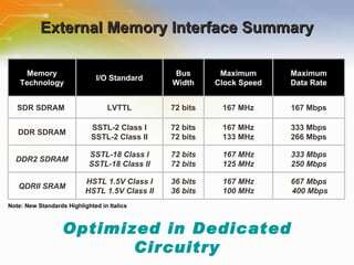
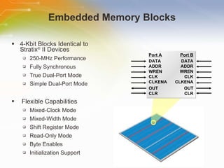
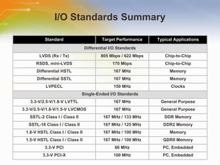
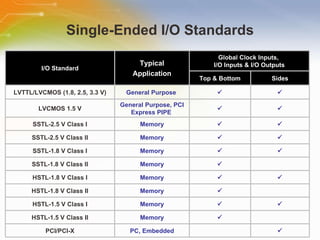
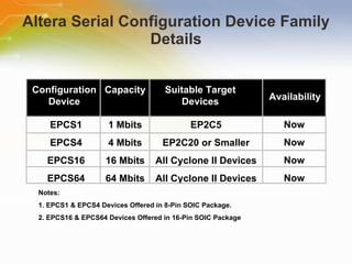
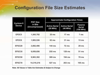
Define Width and Height of Core and Die (http://www.vlsisystemdesign.com/PD-F...VLSI SYSTEM Design
https://www.udemy.com/vlsi-academy
The very first step in chip design is floorplanning, in which the width and height of the chip, basically the area of the chip, is defined. A chip consists of two parts, 'core' and 'die'.
Synthesis in VLSI is the process of converting your code (program) into a circuit. In terms of logic gates, synthesis is the process of translating an abstract design into a properly implemented chip. Hardware Description Languages (HDLs) are specific programming languages that are used to explain the hardware of a circuit, and the computer subsequently builds the circuit depending on the programme you provided. A “Gate Level Netlist” is what you get once you finish synthesising. This is how your circuit will appear. It demonstrates how everything is interconnected. You can alter it if you like; the computer just synthesizes this netlist based on its best judgement. The synthesizer generates better netlists as the abilities improve and they become more proficient at creating HDL programmes.
Presentation on various logic families like RTL, DTL, TTL, IIL etc with diagram, advantages and limitations plus some basic concepts like fan out, noise margin, propagation delay.
Fusion Compiler is the next-generation RTL-to-GDSII implementation system architected to address the complexities of advanced node designs and deliver up to 20% improved PPA while reducing Time To Results (TTR) by 2X.
Gate Diffusion Input Technology (Very Large Scale Integration)Ashwin Shroff
The aim of project is by using GDI technique the power consumption, delay, chip area and connection and parasitic capacitors is decreased. In this project, we are implementing the new T-flip flop using GDI technique for low power and high speed in order to achieve power delay product (PDP)
A VLSI (Very Large Scale Integration) system integrates millions of “electronic components” in a small area (few mm2 few cm2).
design “efficient” VLSI systems that has:
Circuit Speed ( high )
Power consumption ( low )
Design Area ( low )
The CMOS VLSI DESIGN PPT had the complete vision on VLSI Design styles in chip fabrication. It can give a good amount of knowledge to the students who needs VLSI Design
In the world of Very Large Scale Integration (VLSI), the Physical Design process plays a crucial role in transforming a logical design into a physical layout that can be manufactured. Among the various steps involved in the Physical Design flow, Place and Route (PnR) stand out as a critical phase. PnR consists in placing the different components of a design on a chip and routing the connections between them. In this article, we will delve into the PnR flow, exploring its key steps, challenges, and the tools involved.
1. Partitioning:
Partitioning is a preliminary step in the PnR flow that divides the design into manageable blocks or modules based on functionality, hierarchy, or timing constraints. It enables parallel processing during subsequent steps and facilitates easier placement and routing. Partitioning algorithms aim to balance the workload across partitions and minimize inter-partition communication.
2. Floorplanning:
Floorplanning is a critical aspect of the placement process, defining the overall chip's top-level structure and organizing the different functional blocks. It involves allocating space for each block, determining their relative positions, and defining the placement regions. Effective floorplanning ensures proper utilization of available chip areas, reduces congestion, and facilitates efficient routing.
3. Power Planning:
Power planning focuses on distributing power supply and ensuring a stable power delivery network throughout the chip. It involves inserting power distribution networks, decoupling capacitors, and voltage regulators to minimize voltage drop, signal noise, and power supply fluctuations. Power planning techniques aim to optimize power grid layout, reduce IR drop, and mitigate electromigration issues.
4. Placement:
Placement is the first step in the PnR flow and involves determining the optimal location for each logic component on the chip. The primary objective of placement is to minimize wire length, power consumption, and timing delays while adhering to various constraints such as blockages, power grid, and signal integrity.
5. Clock Tree Synthesis (CTS):
Clock Tree Synthesis is a crucial step in PnR flow that ensures the efficient distribution of clock signals to all sequential elements of the design. CTS aims to minimize clock skew, and power dissipation, and provide a balanced clock network. CTS algorithms construct a tree-like structure by inserting buffers and optimizing wire length to achieve reliable clock distribution.
6. Routing:
6.1 Global Routing:
Once the placement is complete, the next step is global routing, which establishes the connections between the placed components. Global routing generates a coarse routing structure using minimum spanning trees, maze routing, or other algorithms. It focuses on achieving reasonable wirelength and reducing congestion without considering the precise details of the interconnects.
This is the presentation that was shared by Nilesh Ranpura and Vineeth Mathramkote at CDNLIVE 2015. The session briefs about the implementation challenges and covers the solution approach and how to achieve results
DesignCon 2019 112-Gbps Electrical Interfaces: An OIF Update on CEI-112GLeah Wilkinson
DesignCon 2019
112-Gbps Electrical Interfaces: An OIF Update on CEI-112G
Brian Holden, Kandou Bus
Cathy Liu, Broadcom
Steve Sekel, Keysight
Nathan Tracy, TE Connectivity
I have prepared it to create an understanding of delay modeling in VLSI.
Regards,
Vishal Sharma
Doctoral Research Scholar,
IIT Indore
vishalfzd@gmail.com
Various processor architectures are described in this presentation. It could be useful for people working for h/w selection and processor identification.
RiseTime offers "Job Oriented VLSI Design & Verification Course"
In this course, you will learn both ASIC design and verification concepts. Verilog is covered as part of design and systemVerilog/UVM are covered as part of verification. The course highlights are periodical tests followed by extensive lab sessions and mock interviews.
A summarised presentation of a study conducted by Cam Leitch and Shane Holborn for the Queensland Australia nursery industry investigating damage from cyclones (hurricanes) and high wind events.
High Fidelity Wind Model Software for Real-Time Simulation PlatformsSimspace Ingeniería SL
A High Fidelity Wind Model Software for Real-Time Simulation Platforms was published and presented for the first time at the 2015 I/ITSEC. I/ITSEC is the The World’s Largest Modeling & Training Conference.
The MYC-CZU3EG CPU Module is a powerful MPSoC System-on-Module (SoM) based on Xilinx Zynq UltraScale+ ZU3EG which features a 1.2 GHz quad-core ARM Cortex-A53 64-bit application processor
this presentation is a great to deliver in classrooms, stage or also can be used to deliver lecture on "Evolution of processor".
it is also very helpful to learn about microprocessor, directly we can say its a self pack containing all about microprocessor.
this ppt contains evolution not only on the basis of generations but also on the basis of their invention.
must gothrough it
The MYC-C7Z015 CPU Module is an SOM (System on Module) board based on Xilinx XC7Z015 (Z-7015) All Programmable System-on-Chip (SoC) which is among the Xilinx Zynq-7000 family, featuring integrated dual-core ARM Cortex-A9 processor with Xilinx 7-series FPGA logic, four 6.25Gbps SerDes transceivers and one PCIe Gen2 x 4 integrated block. The MYC-C7Z015 module has 1GB DDR3 SDRAM, 4GB eMMC, 32MB quad SPI Flash, a Gigabit Ethernet PHY, a USB PHY and external watchdog on board. It provides a large number of I/O signals for ARM peripherals and FPGA I/Os through two 0.8mm pitch 140-pin board-to-board connectors, which is ideal for your next embedded design.
The MYC-C7Z015 CPU Module is compatible with MYIR’s MYC-C7Z010/20 CPU Modules and they can share the same base board which is designed by MYIR for evaluation or prototype purpose. The MYD-C7Z015 development board takes full features of the Zynq-7015 SoC. It has full features of the MYD-C7Z010/20 development board, additionally, it has one PCIe interface and one SFP transceiver module interface.
The MYC-C7Z015 CPU Module is ready to run Linux 3.15.0. It can be used in a variety of commercial, medical, automation, industrial, and military embedded applications.
MYC-Y6ULX CPU Module - NXP i.MX 6UL/6ULL System-on-ModuleLinda Zhang
This overview document gives a brief introduction of MYIR's MYC-Y6ULX CPU Module which is powered by NXP i.MX 6UltraLite / 6ULL processor based on the ARM Cortex-A7 architecture. It is ready to run Linux and delivers high performance with ultra-efficient power that targets Industry Control, Communications, HMI, Smart Healthcare and Internet of Things (IoT) applications. It carries out as many as peripheral signals and IOs through 1.0mm pitch 140-pin stamp hole expansion interface to allow customer’s extension for their next embedded design. The module can support industrial operating temperature range from -40 to +85 Celsius.
MYS-6ULX Single Board Computer for Industry 4.0 and IoT ApplicationsLinda Zhang
The document introduced MYIR's i.MX 6UL / 6ULL based ARM Cortex-A7 Single Board Computer for Industry 4.0 and IoT applications which is ready to run Linux with high performance and ulta low cost.
MYC-YF13X CPU Module - STM32MP135 based SoMLinda Zhang
The MYC-YF13X CPU Module Overview gives introduction of the STM32MP135 processor based System-on-Module from MYIR, a Chinese company focused on providing SoM solutions for embedded appilcations. Measuring only 37mm by 39mm, the MYC-YF13X module has integrated the STM32MP135DAF7 processor, DDR3L, external memory and carried out a variety of peripheral and IO signals through the 1.0 mm pitch 148-pin Castellated-Hole expansion interface. It is capable of running Linux and provided with software resources including kernel and driver source code, together with detailed user manual and documentations to help customer start their development rapidly. It is particularly suitable for applications such as entry-level industrial human-machine interfaces (HMI) and embedded devices for energy and power management.
MYIR also provides the MYD-YF13X Development Board as a starter kit for evaluating the MYC-YF13X CPU Module. It has a versatile base board to facilitate the expansion from the MYC-YF13X through the 1.0 mm pitch 148-pin stamp-hole (Castellated-Hole) interface, a rich set of peripherals and interfaces have been brought out such as RS232, RS485, two USB 2.0 HOST and one USB 2.0 OTG, two Gigabit Ethernet, CAN, one Micro SD card slot, one USB based Mini-PCIe 4G Module interface with one SIM card holder, LCD interface, Camera interface, Audio input and output as well as two extension headers.
More information about the MYC-YF13X CPU Module can be found at:
https://www.myirtech.com/list.asp?id=726
UiPath Test Automation using UiPath Test Suite series, part 3DianaGray10
Welcome to UiPath Test Automation using UiPath Test Suite series part 3. In this session, we will cover desktop automation along with UI automation.
Topics covered:
UI automation Introduction,
UI automation Sample
Desktop automation flow
Pradeep Chinnala, Senior Consultant Automation Developer @WonderBotz and UiPath MVP
Deepak Rai, Automation Practice Lead, Boundaryless Group and UiPath MVP
JMeter webinar - integration with InfluxDB and GrafanaRTTS
Watch this recorded webinar about real-time monitoring of application performance. See how to integrate Apache JMeter, the open-source leader in performance testing, with InfluxDB, the open-source time-series database, and Grafana, the open-source analytics and visualization application.
In this webinar, we will review the benefits of leveraging InfluxDB and Grafana when executing load tests and demonstrate how these tools are used to visualize performance metrics.
Length: 30 minutes
Session Overview
-------------------------------------------
During this webinar, we will cover the following topics while demonstrating the integrations of JMeter, InfluxDB and Grafana:
- What out-of-the-box solutions are available for real-time monitoring JMeter tests?
- What are the benefits of integrating InfluxDB and Grafana into the load testing stack?
- Which features are provided by Grafana?
- Demonstration of InfluxDB and Grafana using a practice web application
To view the webinar recording, go to:
https://www.rttsweb.com/jmeter-integration-webinar
Generating a custom Ruby SDK for your web service or Rails API using Smithyg2nightmarescribd
Have you ever wanted a Ruby client API to communicate with your web service? Smithy is a protocol-agnostic language for defining services and SDKs. Smithy Ruby is an implementation of Smithy that generates a Ruby SDK using a Smithy model. In this talk, we will explore Smithy and Smithy Ruby to learn how to generate custom feature-rich SDKs that can communicate with any web service, such as a Rails JSON API.
Encryption in Microsoft 365 - ExpertsLive Netherlands 2024Albert Hoitingh
In this session I delve into the encryption technology used in Microsoft 365 and Microsoft Purview. Including the concepts of Customer Key and Double Key Encryption.
Dev Dives: Train smarter, not harder – active learning and UiPath LLMs for do...UiPathCommunity
💥 Speed, accuracy, and scaling – discover the superpowers of GenAI in action with UiPath Document Understanding and Communications Mining™:
See how to accelerate model training and optimize model performance with active learning
Learn about the latest enhancements to out-of-the-box document processing – with little to no training required
Get an exclusive demo of the new family of UiPath LLMs – GenAI models specialized for processing different types of documents and messages
This is a hands-on session specifically designed for automation developers and AI enthusiasts seeking to enhance their knowledge in leveraging the latest intelligent document processing capabilities offered by UiPath.
Speakers:
👨🏫 Andras Palfi, Senior Product Manager, UiPath
👩🏫 Lenka Dulovicova, Product Program Manager, UiPath
Securing your Kubernetes cluster_ a step-by-step guide to success !KatiaHIMEUR1
Today, after several years of existence, an extremely active community and an ultra-dynamic ecosystem, Kubernetes has established itself as the de facto standard in container orchestration. Thanks to a wide range of managed services, it has never been so easy to set up a ready-to-use Kubernetes cluster.
However, this ease of use means that the subject of security in Kubernetes is often left for later, or even neglected. This exposes companies to significant risks.
In this talk, I'll show you step-by-step how to secure your Kubernetes cluster for greater peace of mind and reliability.
Connector Corner: Automate dynamic content and events by pushing a buttonDianaGray10
Here is something new! In our next Connector Corner webinar, we will demonstrate how you can use a single workflow to:
Create a campaign using Mailchimp with merge tags/fields
Send an interactive Slack channel message (using buttons)
Have the message received by managers and peers along with a test email for review
But there’s more:
In a second workflow supporting the same use case, you’ll see:
Your campaign sent to target colleagues for approval
If the “Approve” button is clicked, a Jira/Zendesk ticket is created for the marketing design team
But—if the “Reject” button is pushed, colleagues will be alerted via Slack message
Join us to learn more about this new, human-in-the-loop capability, brought to you by Integration Service connectors.
And...
Speakers:
Akshay Agnihotri, Product Manager
Charlie Greenberg, Host
Transcript: Selling digital books in 2024: Insights from industry leaders - T...BookNet Canada
The publishing industry has been selling digital audiobooks and ebooks for over a decade and has found its groove. What’s changed? What has stayed the same? Where do we go from here? Join a group of leading sales peers from across the industry for a conversation about the lessons learned since the popularization of digital books, best practices, digital book supply chain management, and more.
Link to video recording: https://bnctechforum.ca/sessions/selling-digital-books-in-2024-insights-from-industry-leaders/
Presented by BookNet Canada on May 28, 2024, with support from the Department of Canadian Heritage.
State of ICS and IoT Cyber Threat Landscape Report 2024 previewPrayukth K V
The IoT and OT threat landscape report has been prepared by the Threat Research Team at Sectrio using data from Sectrio, cyber threat intelligence farming facilities spread across over 85 cities around the world. In addition, Sectrio also runs AI-based advanced threat and payload engagement facilities that serve as sinks to attract and engage sophisticated threat actors, and newer malware including new variants and latent threats that are at an earlier stage of development.
The latest edition of the OT/ICS and IoT security Threat Landscape Report 2024 also covers:
State of global ICS asset and network exposure
Sectoral targets and attacks as well as the cost of ransom
Global APT activity, AI usage, actor and tactic profiles, and implications
Rise in volumes of AI-powered cyberattacks
Major cyber events in 2024
Malware and malicious payload trends
Cyberattack types and targets
Vulnerability exploit attempts on CVEs
Attacks on counties – USA
Expansion of bot farms – how, where, and why
In-depth analysis of the cyber threat landscape across North America, South America, Europe, APAC, and the Middle East
Why are attacks on smart factories rising?
Cyber risk predictions
Axis of attacks – Europe
Systemic attacks in the Middle East
Download the full report from here:
https://sectrio.com/resources/ot-threat-landscape-reports/sectrio-releases-ot-ics-and-iot-security-threat-landscape-report-2024/
Essentials of Automations: Optimizing FME Workflows with ParametersSafe Software
Are you looking to streamline your workflows and boost your projects’ efficiency? Do you find yourself searching for ways to add flexibility and control over your FME workflows? If so, you’re in the right place.
Join us for an insightful dive into the world of FME parameters, a critical element in optimizing workflow efficiency. This webinar marks the beginning of our three-part “Essentials of Automation” series. This first webinar is designed to equip you with the knowledge and skills to utilize parameters effectively: enhancing the flexibility, maintainability, and user control of your FME projects.
Here’s what you’ll gain:
- Essentials of FME Parameters: Understand the pivotal role of parameters, including Reader/Writer, Transformer, User, and FME Flow categories. Discover how they are the key to unlocking automation and optimization within your workflows.
- Practical Applications in FME Form: Delve into key user parameter types including choice, connections, and file URLs. Allow users to control how a workflow runs, making your workflows more reusable. Learn to import values and deliver the best user experience for your workflows while enhancing accuracy.
- Optimization Strategies in FME Flow: Explore the creation and strategic deployment of parameters in FME Flow, including the use of deployment and geometry parameters, to maximize workflow efficiency.
- Pro Tips for Success: Gain insights on parameterizing connections and leveraging new features like Conditional Visibility for clarity and simplicity.
We’ll wrap up with a glimpse into future webinars, followed by a Q&A session to address your specific questions surrounding this topic.
Don’t miss this opportunity to elevate your FME expertise and drive your projects to new heights of efficiency.
Neuro-symbolic is not enough, we need neuro-*semantic*Frank van Harmelen
Neuro-symbolic (NeSy) AI is on the rise. However, simply machine learning on just any symbolic structure is not sufficient to really harvest the gains of NeSy. These will only be gained when the symbolic structures have an actual semantics. I give an operational definition of semantics as “predictable inference”.
All of this illustrated with link prediction over knowledge graphs, but the argument is general.
Neuro-symbolic is not enough, we need neuro-*semantic*
Cyclone II FPGA Overview
1.
2.
3.
4.
5. Altera product lineup High-end FPGAs with transceiver options CPLDs ASICs Low-cost FPGAs Design software Intellectual property (IP) Development kits Programmable logic solutions for all your needs Low-cost protocol-optimized FPGAs Embedded soft-core processors
6.
7.
8. Cyclone II Family Overview Note: All Densities Will be Offered in All Speed Grades (-6, -7, -8). -6 is the Fastest Speed Grade. Device Logic Elements M4K Memory Blocks Total Memory Bits 18x18 Embedded Multipliers PLLs Maximum User I/O Pins EP2C5 4,608 26 119,808 13 2 142 EP2C8 8,256 36 165,888 18 2 182 EP2C20 18,752 52 239,616 26 4 315 EP2C35 33,216 105 483,840 35 4 475 EP2C50 50,528 129 594,432 86 4 450 EP2C70 68,416 250 1,152,000 150 4 622
9. Cyclone II Packaging & User I/O Denotes Vertical Migration Support Note: (1) This device will be supported in the Quartus ® II version 5.0 software. (2) This device offers 299 user I/Os when vertical migration is enabled with the EP2C35. The 16 user I/Os in the EP2C20F484 become power and ground pins in the EP2C35F484 to support the core. Device 144-Pin TQFP 0.5 mm 22 x 22 208-Pin PQFP 0.5 mm 30.6 x30.6 256-Pin FBGA 1.0 mm 17 x 17 484-Pin FBGA 1.0 mm 23 x 23 672-Pin FBGA 1.0 mm 27 x 27 896-Pin FBGA 1.0 mm 31 x 31 EP2C5 89 142 158 (1) EP2C8 85 138 182 EP2C20 152 315 (2) EP2C35 322 475 EP2C50 294 450 EP2C70 422 622
10.
11. Soft-Core Processor Available Programmable Logic Available Programmable Logic (1) Based on the Nios II fast core. (2) Based on the Nios II economy core. Device EP1C20 EP2C20 Performance 50 DMIPs 100 DMIPs (1) Logic Element Usage 1,200 LEs (Nios) 550 LEs (Nios II) (2) % of Device 6% 3% Cost of Nios $1.20 (Nios) $0.35 (Nios II)
12.
13. EP2C35 Device Floorplan Logic Array M4K Memory Blocks Embedded Multipliers Phase-Locked Loops Side I/O Elements with Support for PCI/PCI-X & Memory Interfaces Top & Bottom I/O Elements with Support for Memory Interfaces
15. Cyclone II Logic Element LUT In1 In2 In3 In4 Carry In0 Carry In1 Carry Out0 Carry Out1 LUT Chain Register Chain General Routing Local Routing General Routing Register Chain Clock REG
16. Embedded Multiplier Details 18 Sign_X 18 X Y Sign_Y Input Registers 36 Clock Clear 36 Output Registers Note: Fastest Speed Grade with Registers Activated in 18x18 or 9x9 Mode 250-MHz Performance
17.
18. External Memory Interface Summary Optimized in Dedicated Circuitry Note: New Standards Highlighted in Italics Memory Technology I/O Standard Bus Width Maximum Clock Speed Maximum Data Rate SDR SDRAM LVTTL 72 bits 167 MHz 167 Mbps DDR SDRAM SSTL-2 Class I SSTL-2 Class II 72 bits 72 bits 167 MHz 133 MHz 333 Mbps 266 Mbps DDR2 SDRAM SSTL-18 Class I SSTL-18 Class II 72 bits 72 bits 167 MHz 125 MHz 333 Mbps 250 Mbps QDRII SRAM HSTL 1.5V Class I HSTL 1.5V Class II 36 bits 36 bits 167 MHz 100 MHz 667 Mbps 400 Mbps
19.
20. I/O Standards Summary Standard Target Performance Typical Applications Differential I/O Standards LVDS (Rx / Tx) 805 Mbps / 622 Mbps Chip-to-Chip RSDS, mini-LVDS 170 Mbps Chip-to-Chip Differential HSTL 167 MHz Memory Differential SSTL 167 MHz Memory LVPECL 150 MHz Clocks Single-Ended I/O Standards 3.3-V/2.5-V/1.8-V LVTTL 167 MHz General Purpose 3.3-V/2.5-V/1.8-V/1.5-V LVCMOS 167 MHz General Purpose SSTL-2 Class I / Class II 167 MHz / 133 MHz DDR Memory SSTL-18 Class I / Class II 167 MHz / 125 MHz DDR2 Memory 1.8-V HSTL Class I / Class II 167 MHz / 100 MHz Memory 1.5-V HSTL Class I / Class II 167 MHz / 100 MHz QDRII Memory 3.3-V PCI 66 MHz PC, Embedded 3.3-V PCI-X 100 MHz PC, Embedded
21. Single-Ended I/O Standards I/O Standard Typical Application Global Clock Inputs, I/O Inputs & I/O Outputs Top & Bottom Sides LVTTL/LVCMOS (1.8, 2.5, 3.3 V) General Purpose LVCMOS 1.5 V General Purpose, PCI Express PIPE SSTL-2.5 V Class I Memory SSTL-2.5 V Class II Memory SSTL-1.8 V Class I Memory SSTL-1.8 V Class II Memory HSTL-1.8 V Class I Memory HSTL-1.8 V Class II Memory HSTL-1.5 V Class I Memory HSTL-1.5 V Class II Memory PCI/PCI-X PC, Embedded
22. Differential I/O Standards I/O Standard Global Clock Inputs I/O Inputs I/O Outputs Top & Bottom Sides Top & Bottom Sides Top & Bottom Sides SSTL-2.5 V Class I SSTL-2.5 V Class II SSTL-1.8 V Class I SSTL-1.8 V Class II HSTL-1.8 V Class I HSTL-1.8 V Class II HSTL-1.5 V Class I HSTL-1.5 V Class II LVDS Mini LVDS RSDS LVPECL
23. I/O Element Structure Pin Output Enable Data Out Reg Output Clock Clock Data In Reg Data In Comb Data Out Comb REG REG REG
24. Programmable Drive Strength I/O Standard IOH/IOL Current Strength Setting (mA) LVTTL/LVCMOS (3.3 V) 4, 8, 12, 16, 20, 24 LVTTL/LVCMOS (2.5 V) 4, 8, 12, 16 LVTTL/LVCMOS (1.8 V) 2, 4, 6, 8, 10, 12 LVCMOS 1.5 V 2, 4, 6, 8 SSTL-2 Class I 8, 12 SSTL-2 Class II 16, 20, 24 SSTL-18 Class I 4, 6, 8, 10, 12 SSTL-18 Class II 8, 16, 18 HSTL-18 Class I 4, 6, 8, 10, 12 HSTL-18 Class II 16, 18, 20 HSTL-15 Class I 4, 6, 8, 10, 12 HSTL-15 Class II 16
25.
26. I/O Bank Numbers & Locations EP2C5 to EP2C8 2 1 4 3 EP2C20 to EP2C70 3 4 8 7 2 1 5 6
27. PLL Parameters & Locations Cyclone II 3 2 1 4 PLL EP2C5 EP2C8 EP2C20 EP2C35 EP2C50 EP2C70 1 2 3 4 Parameter Cyclone II PLL Input Frequency Range 11 to 311 MHz Output Frequency Range 10 to 402.5 MHz Time to Lock from Power up 1 ms VCO Operating Range 300 MHz to 1 GHz
28. Altera Serial Configuration Device Family Details Notes: 1. EPCS1 & EPCS4 Devices Offered in 8-Pin SOIC Package. 2. EPCS16 & EPCS64 Devices Offered in 16-Pin SOIC Package Availability Availability EPCS1 EPCS4 EPCS16 EPCS64 1 Mbits 4 Mbits 16 Mbits 64 Mbits Configuration Device Capacity EP2C5 EP2C20 or Smaller All Cyclone II Devices All Cyclone II Devices Suitable Target Devices Now Now Now Now
29. Configuration File Size Estimates Note: All Values in Table Are Estimates & Subject to Change Cyclone II Device POF Size in Bits (Uncompressed) Approximate Configuration Times Active Serial (20 MHz) Active Serial (40 MHz) Passive Serial (100 MHz) EP2C5 1,265,792 35 ms 17 ms 7 ms EP2C8 1,983,536 63 ms 31 ms 13 ms EP2C20 3,892,496 144 ms 72 ms 29 ms EP2C35 6,858,656 255 ms 128 ms 51 ms EP2C50 9,963,392 389 ms 194 ms 78 ms EP2C70 14,319,216 527 ms 263 ms 105 ms
30.
31.
Editor's Notes
This is a training module for the Altera Cyclone II FPGA
Welcome to this module on the Cyclone II family FPGA from Altera. The module overviews the major features of the Cyclone II family FPGA.
Programmable logic is loosely defined as a device with configurable logic and flip-flops linked together with programmable resources that control the interconnections. User-programmable memory cells control and define the function that the logic performs and how the various logic functions are interconnected. Thus a wide range of sequential circuits can be implemented on a low-cost PLD. Though various devices use different architectures, all are based on this fundamental idea.
FPGAs have gained rapid acceptance over the past decade because users can apply them to a wide range of applications: random logic, integrating multiple SPLDs, device controllers, communication encoding and filtering, small- to medium-size systems with SRAM blocks, and many more. Another interesting FPGA application is prototyping designs to be implemented in gate arrays by using one or more large FPGAs . An application only beginning development is the use of FPGAs as custom computing machines. This involves using the programmable parts to execute software, rather than compiling the software for execution on a regular CPU.
Altera understands programmable devices are part of a bigger picture, and that true design success requires an array of other tools. To that end, Altera complements the complex programmable logic devices (CPLDs) and field programmable gate arrays (FPGAs) with sophisticated software tools, pre-verified and configurable intellectual property (IP) cores, a soft-core processor – Nios II, development kits, and reference designs. Our comprehensive solution portfolios result in a faster, simplified design process and, in turn, faster time to market and lower development costs. With Altera® solutions, you can undertake your design, confident that you’ll be able to meet your unique application design goals.
Following the immensely successful first-generation Cyclone® device family, Altera® Cyclone II FPGAs extend the low-cost FPGA density range to 68,416 logic elements (LEs) and provide up to 622 usable I/O pins and up to 1.1 Mbits of embedded memory. Cyclone II FPGAs are manufactured on 300-mm wafers using TSMC's 90-nm process to ensure rapid availability and low cost. By minimizing silicon area, Cyclone II devices can support complex digital systems on a single chip at a cost that rivals that of ASICs. Altera’s low-cost FPGAs—Cyclone II FPGAs, offer high performance and the low power consumption.
Altera Cyclone II FPGAs extend the low-cost FPGA density range to 68,416 logic elements (LEs) and provide up to 622 usable I/O pins and up to 1.1 Mbits of embedded memory. Embedded multiplier block can implement up to either two 9 × 9-bit multipliers, or one 18 × 18-bit multiplier with up to 250-MHz performance. Embedded multipliers are arranged in columns across the device. Cyclone II devices support a broad range of external memory interfaces, such as SDR SDRAM, DDR SDRAM, DDR2 SDRAM, and QDRII SRAM. Dedicated clock delay control circuitry allows Cyclone II devices to interface with an external memory device at clock speeds up to 167 MHz/333 Mbps for DDR and DDR2 SDRAM devices and 167 MHz/667 Mbps for QDRII SRAM devices. Each Cyclone II device has up to four PLLs, supporting advanced capabilities such as clock switchover and programmable switchover. These PLLs offer clock multiplication and division, phase shifting, and programmable duty cycle and can be used to minimize clock delay and clock skew, and to reduce or adjust clock-to-out and set-up times.
Altera® Cyclone II FPGAs extend the low-cost FPGA density range to 68,416 logic elements (LEs) and provide up to 622 usable I/O pins and up to 1.1 Mbits of embedded memory. Cyclone II devices include a powerful FPGA feature set optimized for low-cost applications including a wide range of density, memory, embedded multiplier, and packaging options. Cyclone II devices support a wide range of common external memory interfaces and I/O protocols required in low-cost applications.
Vertical migration means that you can migrate to devices whose dedicated pins, configuration pins, and power pins are the same for a given package across device densities. Cyclone II devices support vertical migration within the same package (for example, you can migrate between the EP2C35, EPC50, and EP2C70 devices in the 672-pin FineLine BGA package).
Cyclone II devices support the Nios II embedded processor which allows to implement custom-fit embedded processing solutions. Cyclone II devices can also expand the peripheral set, memory, I/O, or performance of embedded processors. Single or multiple Nios II embedded processors can be designed into a Cyclone II device to provide additional co-processing power or even replace existing embedded processors in your system. Using Cyclone II and Nios II together allow for low-cost, high-performance embedded processing solutions, which allow you to extend your product's life cycle and improve time to market over standard product solutions.
Nios and Nios II are the Soft Processor IP solutions from Altera for Embedded Applications. The table demonstrates the resource utilization or Logic Element usage summary for Nios and Nios II Embedded Processor within Cyclone II FPGAs. Nios II processor adds the advantage in better performance with less silicon utilization and comparatively low Cost.
Altera’s Quartus II Design Software supports all the Cyclone II family Devices. Quartus II software has full integrity with advanced tool Such as SOPC Builder and DSP Builder for Embedded and DSP Applications respectively.
Cyclone® II devices contain a two-dimensional row- and column-based architecture to implement custom logic. Column and row interconnects of varying speeds provide signal interconnects between logic array blocks (LABs), embedded memory blocks, and embedded multipliers.
The logic array consists of LABs, with 16 logic elements (LEs) in each LAB. An LE is a small unit of logic providing efficient implementation of user logic functions. LABs are grouped into rows and columns across the device. Cyclone II devices range in density from 4,608 to 68,416 LEs. Each LAB consists of 16 Les, LAB control signals, LE carry chains, Register chains, and Local interconnect.
The smallest unit of logic in the Cyclone II architecture, the LE, is compact and provides advanced features with efficient logic utilization. Each LE features a four-input look-up table (LUT), which is a function generator that can implement any function of four variables, a programmable register, a carry chain connection, a register chain connection, the ability to drive all types of interconnects: local, row, column, register chain, and direct link interconnects, support for register packing, and support for register feedback.
Cyclone II devices have embedded multiplier blocks optimized for multiplier-intensive digital signal processing (DSP) functions, such as finite impulse response (FIR) filters, fast Fourier transform (FFT) functions, and discrete cosine transform (DCT) functions. The embedded multiplier consists of multiplier block, input and output registers, input and output interfaces. Each Cyclone II device has one to three columns of embedded multipliers that efficiently implement multiplication functions.
Embedded multipliers can operate at up to 250 MHz (for the fastest speed grade) for 18 × 18 and 9 × 9 multiplications when using both input and output registers. An embedded multiplier can be configured to support a single 18 × 18 multiplier for operand widths up to 18 bits. All 18-bit multiplier inputs and results can be registered independently. The multiplier operands can accept signed integers, unsigned integers, or a combination of both. An embedded multiplier can be configured to support two 9 × 9 independent multipliers for operand widths up to 9-bits. Both 9-bit multiplier inputs and results can be registered independently. The multiplier operands can accept signed integers, unsigned integers or a combination of both.
Cyclone® II devices support a broad range of external memory interfaces such as SDR SDRAM, DDR SDRAM, DDR2 SDRAM, and QDRII SRAM. Dedicated clock delay control circuitry allows Cyclone II devices to interface with an external memory device at clock speeds up to 167 MHz/333 Mbps for DDR and DDR2 SDRAM devices and 167 MHz/667 Mbps for QDRII SRAM devices. The easiest way to interface to external memory devices is by using one of the Altera® external memory IP cores, such as DDR2 SDRAM Controller MegaCore® Function, DDR SDRAM Controller MegaCore Function, QDRII SRAM Controller MegaCore Function and OpenCore® Plus evaluations of these cores are available for free to Quartus® II Web Edition software users.
The Cyclone II embedded memory consists of columns of M4K memory blocks. The M4K memory blocks include input registers that synchronize writes and output registers to pipeline designs and improve system performance. The output registers can be bypassed, but input registers cannot. Each M4K block can implement various types of memory with or without parity, including true dual-port, simple dual-port, and single-port RAM, ROM, and first-in first-out (FIFO) buffers.
The proliferation of I/O standards and the need for improved I/O performance have made it critical that low-cost devices have flexible I/O capabilities. Selectable I/O capabilities such as SSTL-18, SSTL-2, and LVDS compatibility allow Cyclone® II devices to connect to other devices on the same printed circuit board (PCB) that may require different operating and I/O voltages. With these aspects of implementation easily manipulated using the Altera® Quartus® II software, the Cyclone II device family allows you to use low cost FPGAs while keeping pace with increasing design complexity.
Cyclone II devices support single-ended I/O standards such as LVTTL, LVCMOS, SSTL-2, SSTL-18, HSTL-18, HSTL-15, PCI, and PCI-X to interface with other on-board devices. Single-ended I/O standards are critical when working with advanced memory devices such as double-data rate (DDR and DDR2) SDRAM and QDRII SRAM devices. The table lists the single-ended I/O standards and target performance supported in Cyclone II devices.
From high-speed backplane applications to high-end switch boxes, low-voltage differential signaling (LVDS) is the technology of choice. LVDS is a low-voltage differential signaling standard, allowing higher noise immunity than single-ended I/O technologies. Its low-voltage swing allows for high-speed data transfers, low power consumption, and reduced electromagnetic interference (EMI).
Cyclone II device IOEs contain a bidirectional I/O buffer and three registers for complete embedded bidirectional single data rate transfer. The IOE contains one input register, one output register, and one output enable register. You canuse the input registers for fast setup times and output registers for fast clock-to-output times. Additionally, you can use the output enable (OE) register for fast clock-to-output enable timing. The IOEs are located in I/O blocks around the periphery of the Cyclone II device. There are up to five IOEs per row I/O block and up to four IOEs per column I/O block (column I/O blocks span two columns). The row I/O blocks drive row, column (only C4 interconnects), or direct link interconnects. The column I/O blocks drive column interconnects.
The output buffer for each Cyclone II device I/O pin has a programmable drive strength control for certain I/O standards. The LVTTL, LVCMOS, SSTL-2 class I and II, SSTL-18 class I and II, HSTL-18 class I and II, and HSTL-1.5 class I and II standards have several levels of drive strength that you can control. Using minimum settings provides signal slew rate control to reduce system noise and signal overshoot. The table shows the possible settings for the I/O standards with drive strength control.
PCI Express is rapidly establishing itself as the successor to PCI, It provides higher performance, increased flexibility, and scalability for next-generation systems without increasing costs, all while maintaining software compatibility with existing PCI applications. Now you can easily design high volume, low-cost PCI Express ×1 solutions today with Cyclone II FPGA (EP2C15 or larger). Cyclone® II devices offer hot socketing (also known as hot plug-in, hot insertion, or hot swap) and power sequencing support without the use of any external devices. You can insert or remove a Cyclone II board in a system during system operation without causing undesirable effects to the board or to the running system bus. The hot-socketing feature lessens the board design difficulty when using Cyclone II devices on printed circuit boards (PCBs) that also contain a mixture of 3.3-, 2.5-, 1.8-, and 1.5-V devices. With the Cyclone II hot-socketing feature, you no longer need to ensure a proper power-up sequence for each device on the board.
The I/O pins on Cyclone II devices are grouped together into I/O banks and each bank has a separate power bus. EP2C5 and EP2C8 devices have four I/O banks (see Figure 2–28), while EP2C20 to ECP2C70 devices have eight I/O banks.Each device I/O pin is associated with one I/O bank. To accommodate voltage-referenced I/O standards, each Cyclone II I/O bank has a VREF bus. Each bank in EP2C5, EP2C8, EP2C15, EP2C20, EP2C35, and EP2C50 devices supports two VREF pins and each bank of EP2C70 supports four VREF pins.
Cyclone® II devices have up to four phase-locked loops (PLLs) that provide robust clock management and synthesis for device clock management, external system clock management, and I/O interfaces. Cyclone II PLLs are versatile and can be used as a zero delay buffer, a jitter attenuator, a low skew fan out buffer, or a frequency synthesizer. Cyclone II PLLs support four clock feedback modes: normal mode, zero delay buffer mode, no compensation mode, and source synchronous mode. Cyclone II PLLs do not have support for external feedback mode. All the supported clock feedback modes allow for multiplication and division, phase shifting, and programmable duty cycle.
In the Active Serial configuration scheme, Cyclone II devices are configured using a serial configuration device. These configuration devices are low-cost devices with non-volatile memory that feature a simple, four-pin interface and a small form factor. These features make serial configuration devices an ideal low-cost configuration solution.
The table shows the approximate uncompressed configuration file sizes for Cyclone II devices. To calculate the amount of storage space required for multiple device configurations, add the file size of each device together.
Cyclone II devices include a powerful FPGA feature set optimized for low-cost applications including a wide range of density, memory, embedded multiplier, and packaging options. The low cost and optimized feature set of Cyclone II FPGAs make them ideal solutions for a wide array of automotive, consumer, communications, video processing, test and measurement, and other end-market solutions.
Thank you for taking the time to view this presentation on Altera Cyclone II Series. If you would like to learn more or go on to purchase some of these devices, you may either click on the part list link, or simple call our sales hotline. For more technical information you may either visit the Altera’s site , or if you would prefer to speak to someone live, please call our hotline number, or even use our ‘live chat’ online facility.