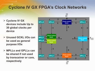
![Cyclone IV E FPGA’s Clock Networks Up to 20 global clocks per device Unused GCKL I/Os can be used as general purpose I/Os GPLL 2 GPLL 4 GPLL 1 GPLL 3 GCLK multiplexer GCLK multiplexer GCLK multiplexer GCLK multiplexer GCLK [14:10] GCLK [9:5] GCLK [15:19] GCLK [0:4] 4 4 4 4](https://image.slidesharecdn.com/alteracyclone-iv-110310202019-phpapp01/85/Cyclone-IV-FPGA-Device-13-320.jpg)

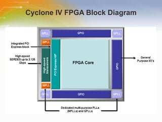
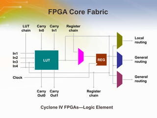
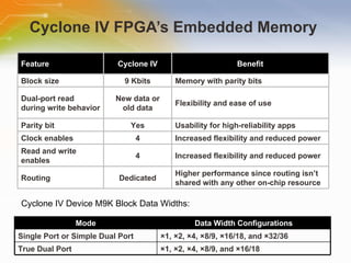
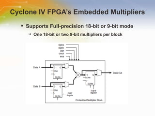
The document provides an overview of Altera's Cyclone IV FPGA family, including features of the Cyclone IV E and GX variants such as logic elements, memory blocks, multipliers, and I/O standards. It describes the core architecture and blocks including the logic fabric, memory interfaces, clock management resources, and transceiver capabilities. Hard IP support for interfaces like PCI Express is also summarized.