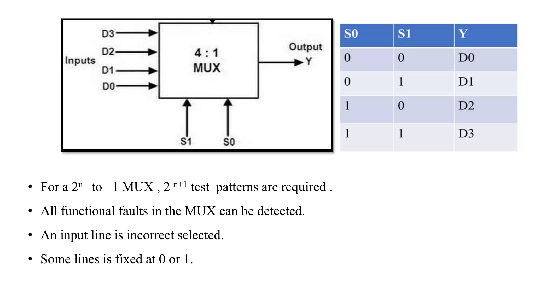
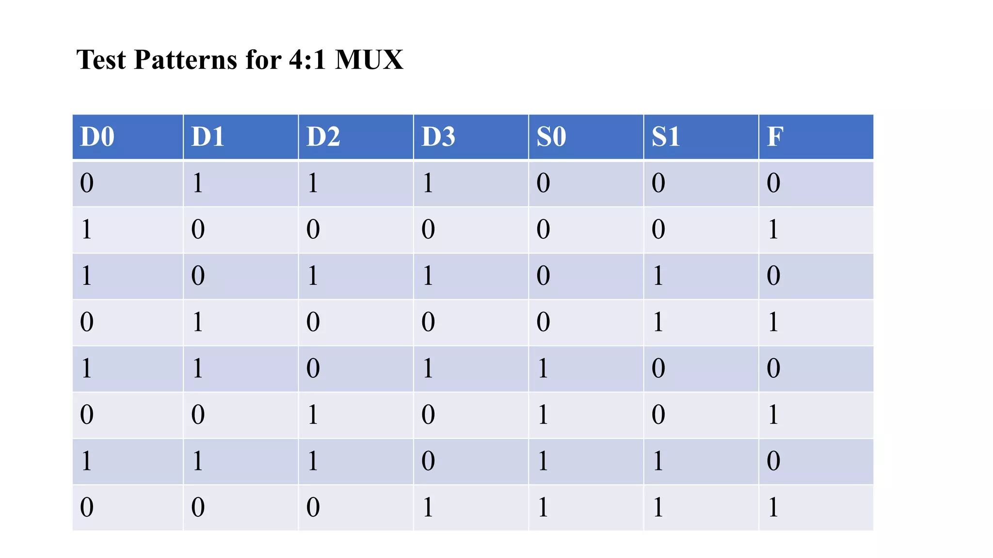
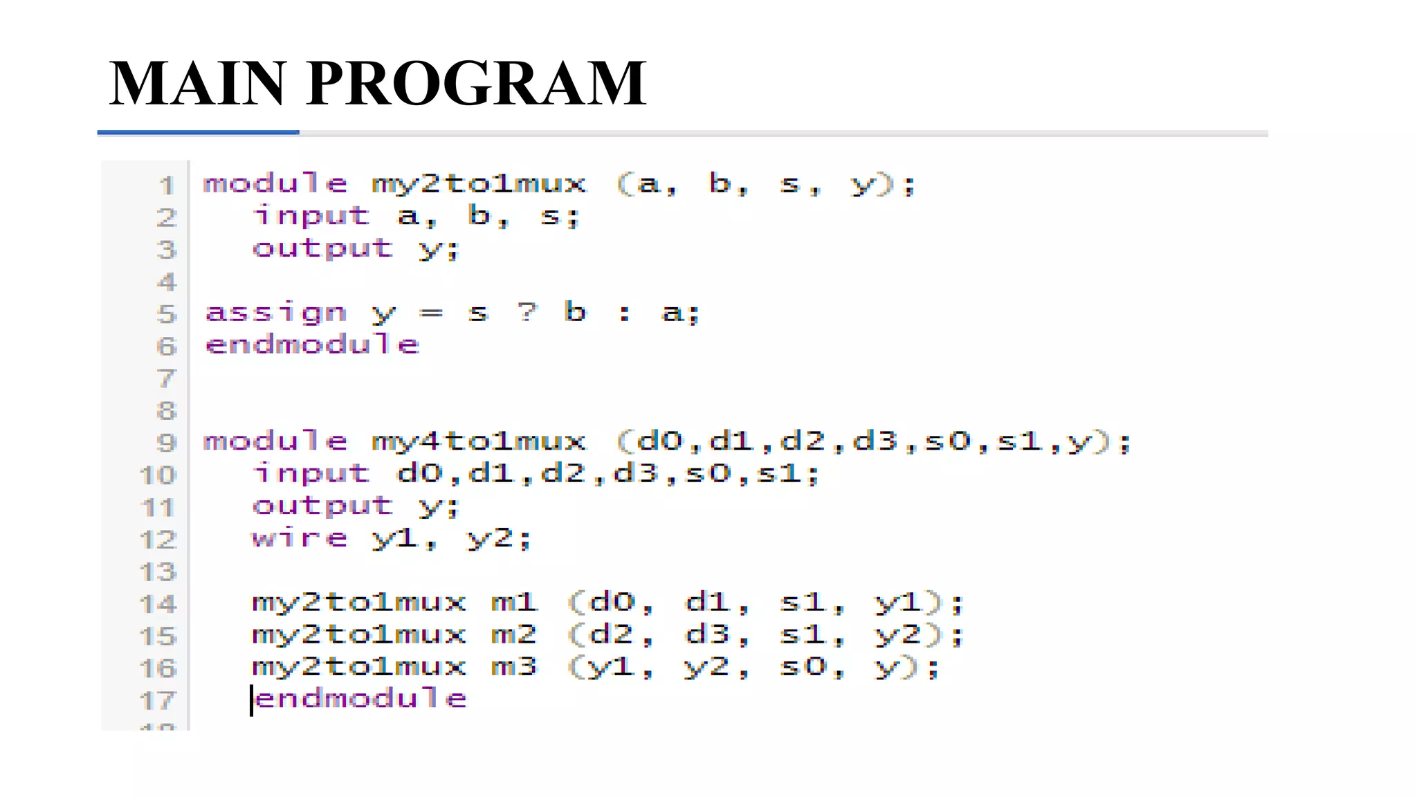
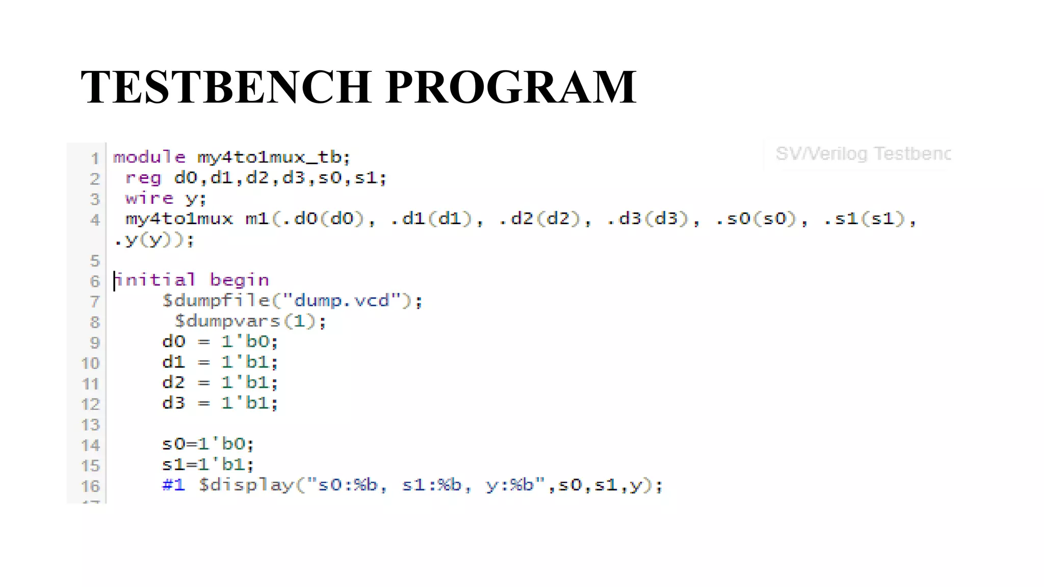
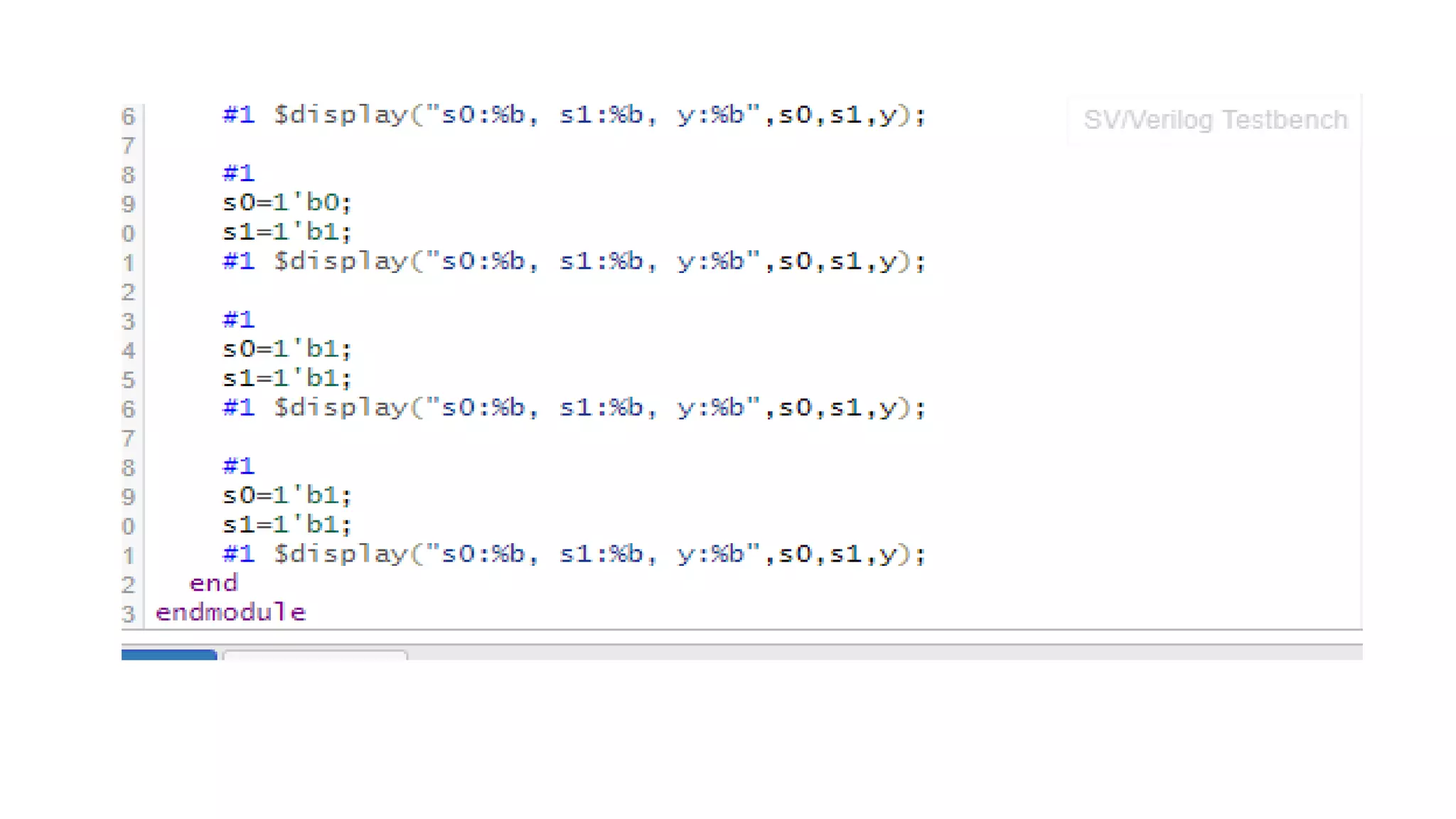
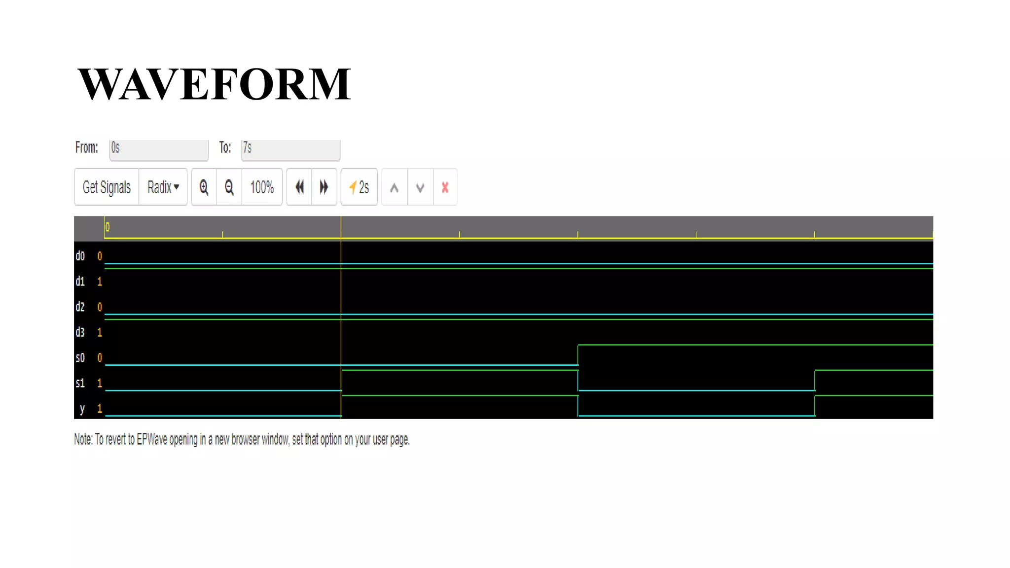
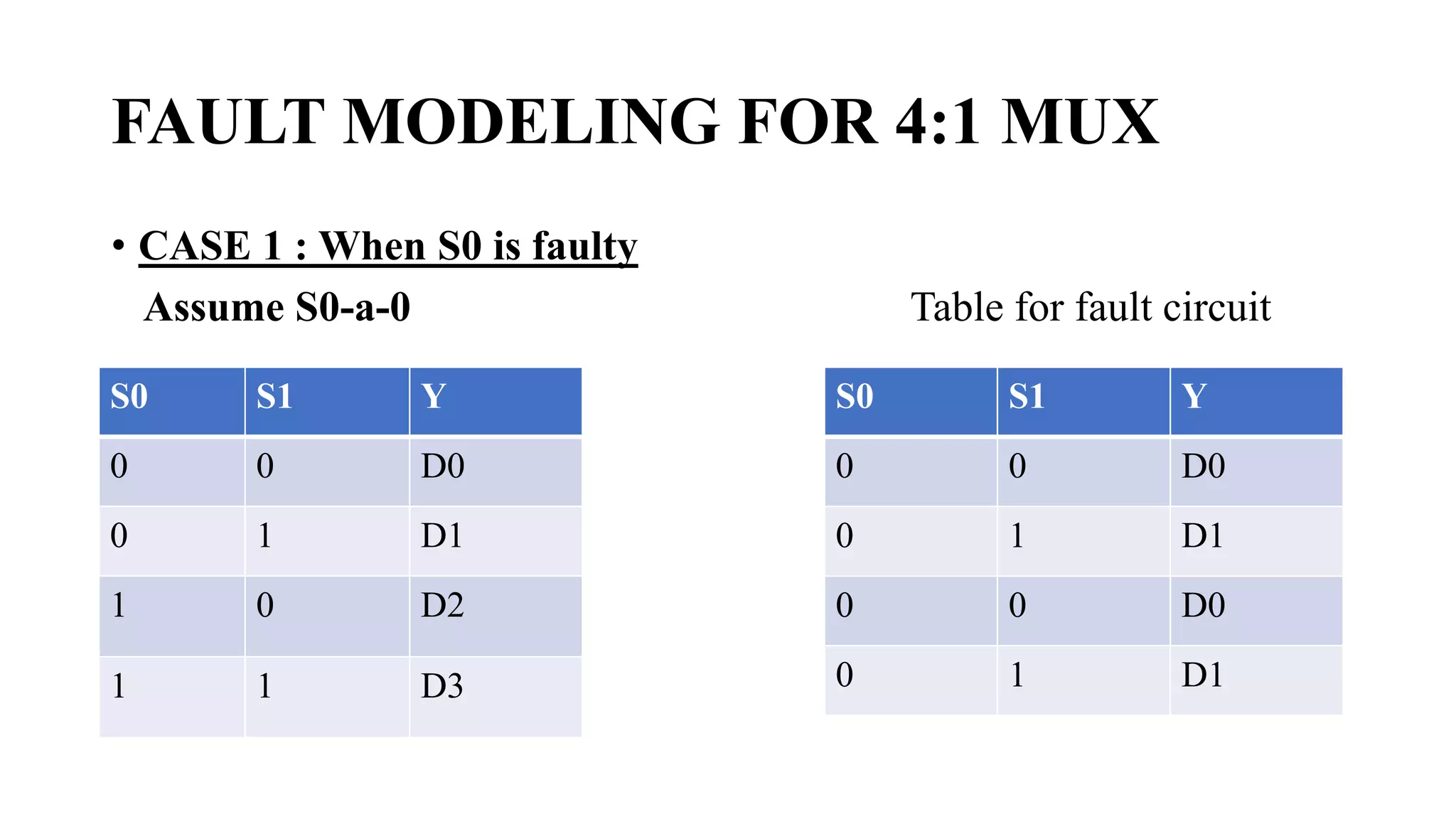
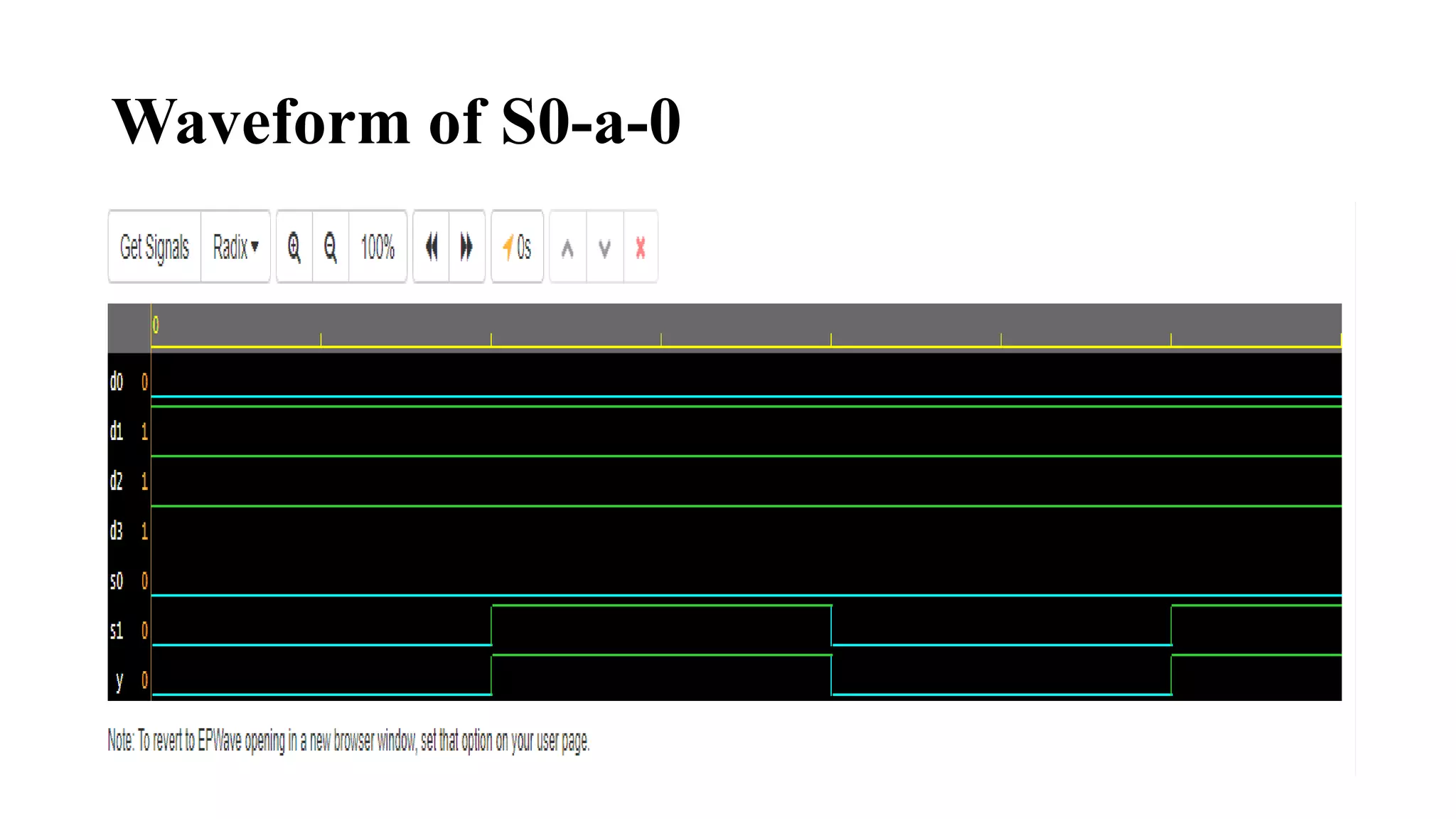
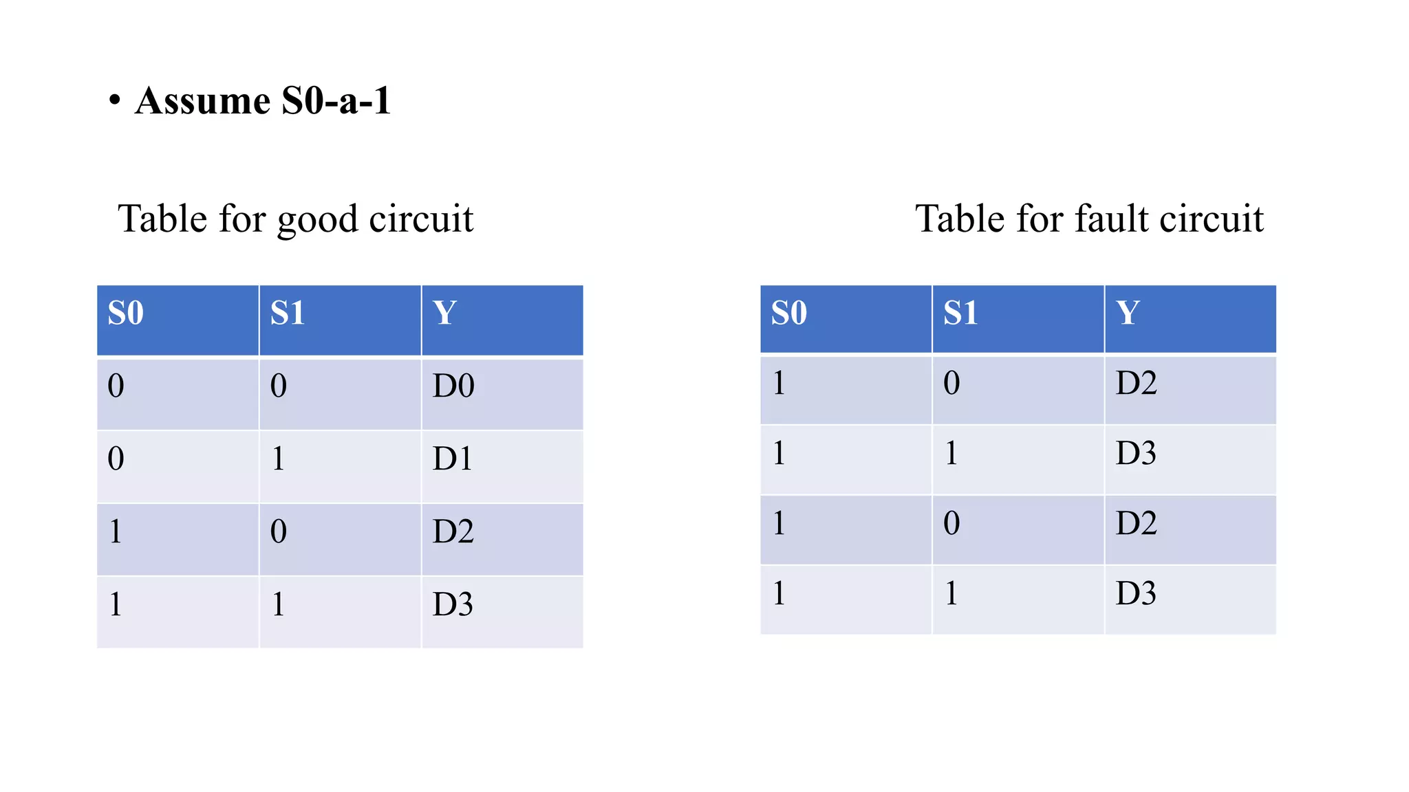
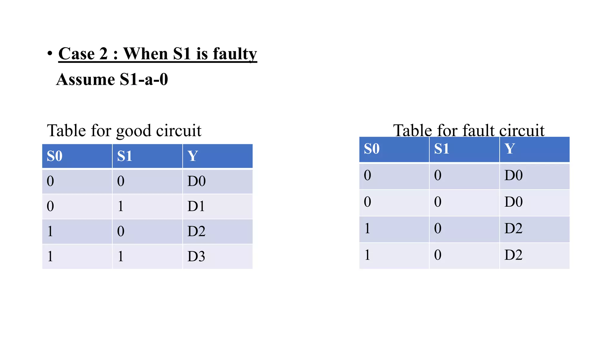
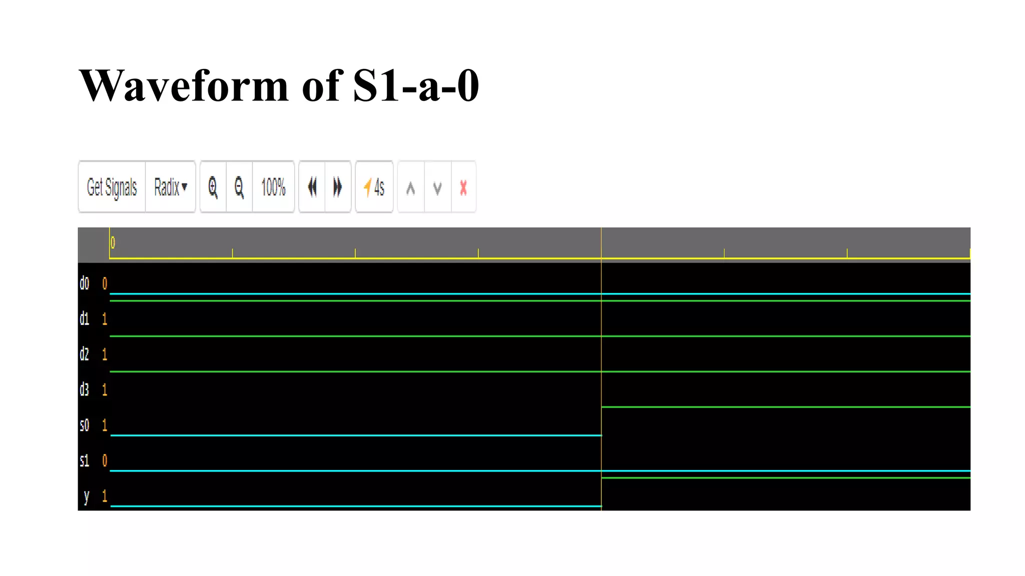
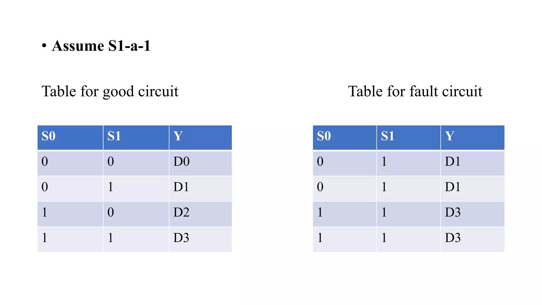
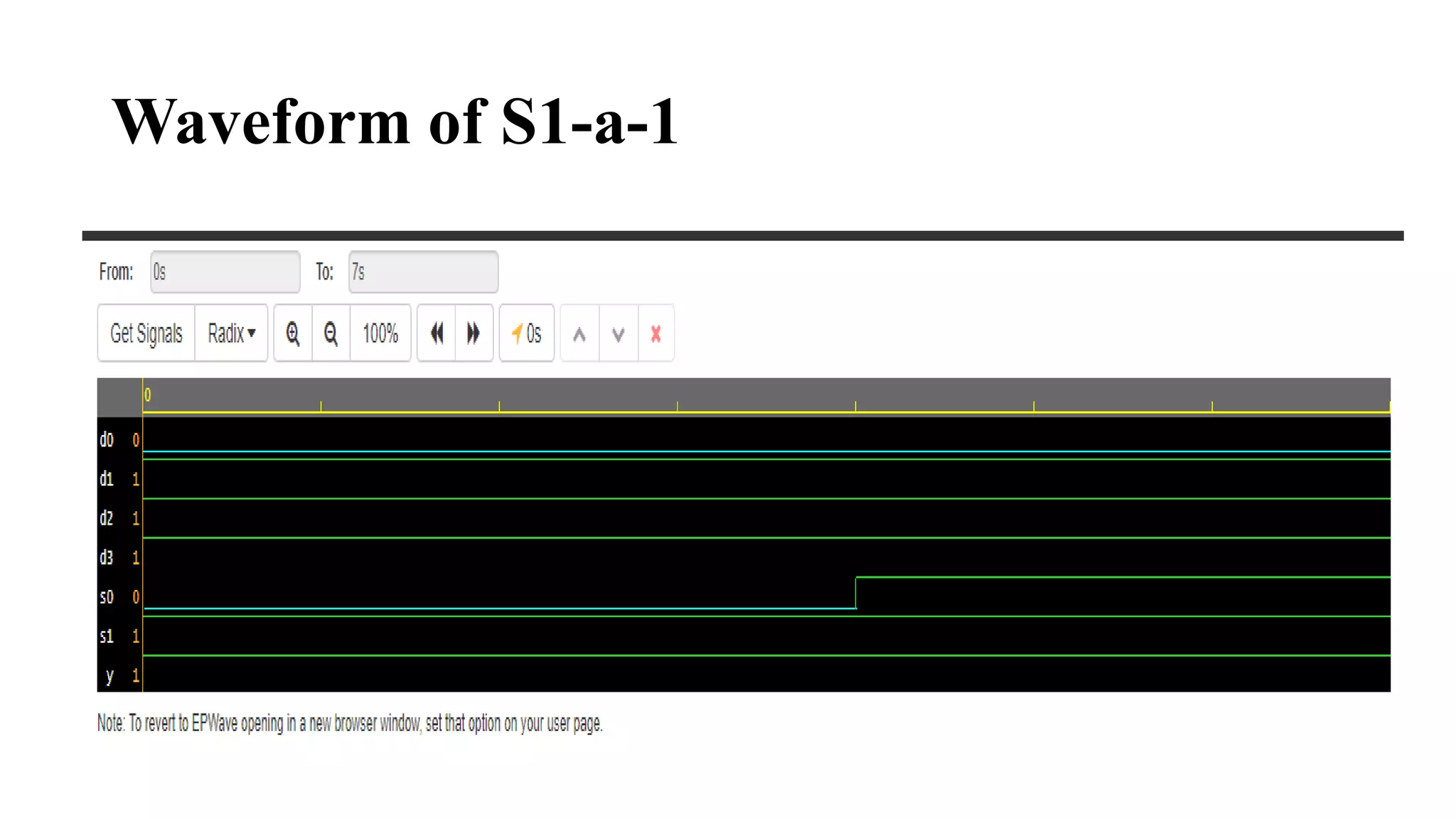
TEST PATTERN GENERATION FOR 4:1
MUX
Presented by
URMILA S
DEPT OF ECE
SJCE MYSURU
TEST PATTERN
• Test pattern generation (TPG) is the process of generating test patterns for a given fault model.
• Automatic Test Pattern Generation, or ATPG, is a process used in semiconductor electronic device
testing wherein the test patterns required to check a device for faults are automatically generated by
a program.
• The generated patterns are used to test semiconductor devices after manufacture, or to assist with
determining the cause of failure (failure analysis).
• The effectiveness of ATPG is measured by the number of modeled defects, or fault models,
detectable and by the number of generated patterns.
• The quality of the test pattern can be evaluated on the basis of the fault coverage.
• Test patterns for large VLSI systems are often determined from the knowledge of the circuit
function.
• A fault simulator is then used to find the effectiveness of the test patterns in detecting gate-level
“stuck-at” faults.
• Existing gate-level fault simulation techniques suffer prohibitively expensive performance
penalties when applied to the modern VLSI systems of larger sizes.
• Post-synthesis findings of such test generation and fault simulation efforts are too late in the design
cycle to be useful for Design-For-Test (DFT) related improvements in the architecture. Therefore,
an effective Register-Transfer Level (RTL) fault model is highly desirable.
ROLE OF TESTING IN VLSI DESIGN
• Even though a circuit is designed error-free, manufactured circuits may not function
correctly. Since the manufacturing process is not perfect, some defects such as short-
circuits, open-circuits, open interconnections, pin shorts, etc., may be introduced.
• It is important to identify a faulty component as early in the manufacturing process as
possible. Therefore, testing has become a very important aspect of any VLSI
manufacturing system.
• The testing of digital logic involves the application of the appropriate stimuli to a Device
Under-Test (DUT) and the comparison of the resulting response to the expected one.
FAULT MODEL ANALYSIS
• The early test generation approaches involved either the creation of all possible combinations for
device inputs or the creation of stimuli targeted to verify certain functional features of the device.
• The application of 2n test vectors to a device with n inputs is effective if n is small and the device does
not contain memory elements.
• An exhaustive test pattern set for a modern VLSI circuit could result into a hundred million or more
vectors. Each circuit is tested for a given set of test patterns using Automatic Test Equipment (ATE).
• In order to reduce the test application cost (which primarily comprises of the tester time and the cost
of test equipment), it is important to keep the number of test patterns to a minimum.
• An efficient test generation approach that targets hardware faults rather than the function. This is done
by creating test patterns for specific faults.
FAULT SIMULATIONAND TEST EVALUATION
• Fault simulation is the process of simulating a circuit with a given set of test patterns and a set of
faults, and comparing the response of the circuit with each fault to that of the fault-free circuit.
• If the response does not match, the fault is considered detected by the given set of test patterns.
• Thus simulation can be used to evaluate or grade test patterns.
• The quality of test patterns is determined by fault coverage, which is a ratio of the number of
detected faults to the total number of simulated faults.
• Fault coverage bears a nonlinear relationship to defect coverage, which is the probability that a test
set detects any physical fault in the circuit.
EDA PLAYGROUND
EDA Playground gives engineers immediate hands-on exposure to simulating and synthesizing
System Verilog, Verilog, VHDL, C++/SystemC, and other HDLs. All you need is a web browser.
• With a simple click, run your code and see console output in real time.
• View waves for your simulation using EPWave browser-based wave viewer.
• Save your code snippets (“Playgrounds”).
• Share your code and simulation results with a web link. Perfect for web forum discussions or
emails. Great for asking questions or sharing your knowledge.
You can run a simulation on EDA Playground and load the resulting waves in EPWave.
The testbench (left editor pane) and design (right editor pane) may be
written using one of these languages:
• Verilog/System Verilog for both
• VHDL for both
• e for testbench, and System Verilog/Verilog for design
• Python for testbench, and System Verilog/Verilog for design
• Python for both
VERILOG
Along with VHDL, Verilog is among the most widely used HDLs.
• Main differences:
– VHDL was designed to support system level design and
specification.
– Verilog was designed primarily for digital hardware designers developing FPGAs
and ASICs.
Concept of Verilog “Module”
• In Verilog, the basic unit of hardware is called a module.
– Modules cannot contain definitions of other modules.
– A module can, however, be instantiated within another module.
– Allows the creation of a hierarchy in a Verilog description.
VARIABLE DATA TYPES
• A variable belongs to one of two data types:
– Net
• Must be continuously driven
• Used to model connections between continuous assignments & instantiations
– Register
• Retains the last value assigned to it
• Often used to represent storage elements
DESCRIPTIONSTYLES IN VERILOG
• Two different styles of description:
1. Data flow
• Continuous assignment
2. Behavioral
• Procedural assignment Blocking Non-blocking
BEHAVIORAL STYLE
Procedural Assignment
• The procedural block defines
– A region of code containing sequential statements.
– The statements execute in the order they are written.
• Two types of procedural blocks in Verilog
– The “always” block
• A continuous loop that never terminates.
– The “initial” block
• Executed once at the beginning of simulation (used in Test-benches).
• A module can contain any number of “always” blocks, all of which execute
concurrently.
• The @(event_expression) is required for both combinational and sequential logic
descriptions.
• Only “reg” type variables can be assigned within an “always” block.
PROPERTIES OF THE GATE LEVEL SSF MODEL :
1) Boolean components are assumed to be fault-free.
2) Signal lines contain faults:
• a stuck-at-zero (s-a-0) fault when the logic level is fixed at value 0
• a stuck-at-one (s-a-1) fault when the logic level is fixed at value
(3) According to the single fault (SSF) assumption, only one fault is applied at a time when a test
set is either being created or evaluated.
(4) The fault-list is collapsed using the “check-point” theorem [ABR90]. The collapsed fault-list
of a module contains input as well as fan-out faults. Further collapsing may be done using
structural equivalence and dominance relationships.
PROPERTIES OF THE RTL FAULT MODEL:
(1) Language operators (which map onto Boolean components in the gate-level netlist) are assumed to be
fault-free.
(2) Variables (which map onto signal lines in the gate-level netlist) contain faults:
• a stuck-at-zero (s-a-0) fault when the logic level is fixed at value 0
• a stuck-at-one (s-a-1) fault when the logic level is fixed at value 1
(3) The proposed RTL fault model follows the single fault assumption and therefore only one fault is
applied at a time when a test set is evaluated.
(4) The RTL fault-list of a module contains input as well as fan-out faults. RTL variables that are used
more than once in executable statements or the instantiations of lower level modules of the design-
hierarchy are considered to have fan-out.
Input faults of a module at the RT level have one-to-one equivalence to input faults of the module at the
gate-level.
FUNCTIONAL LEVEL FAULT MODEL
• For a 2n to 1 MUX , 2 n+1 test patterns are required .
• All functional faults in the MUX can be detected.
• An input line is incorrect selected.
• Some lines is fixed at 0 or 1.
Test Patterns for 4:1 MUX
D0 D1 D2 D3 S0 S1 F
0 1 1 1 0 0 0
1 0 0 0 0 0 1
1 0 1 1 0 1 0
0 1 0 0 0 1 1
1 1 0 1 1 0 0
0 0 1 0 1 0 1
1 1 1 0 1 1 0
0 0 0 1 1 1 1
MAIN PROGRAM
TESTBENCH PROGRAM
WAVEFORM
FAULT MODELING FOR 4:1 MUX
• CASE 1 : When S0 is faulty
Assume S0-a-0 Table for fault circuit
•
S0 S1 Y
0 0 D0
0 1 D1
1 0 D2
1 1 D3
S0 S1 Y
0 0 D0
0 1 D1
0 0 D0
0 1 D1
Waveform of S0-a-0
• Assume S0-a-1
Table for good circuit Table for fault circuit
S0 S1 Y
0 0 D0
0 1 D1
1 0 D2
1 1 D3
S0 S1 Y
1 0 D2
1 1 D3
1 0 D2
1 1 D3
Waveform of S0-a-1
• Case 2 : When S1 is faulty
Assume S1-a-0
Table for good circuit Table for fault circuit
S0 S1 Y
0 0 D0
0 1 D1
1 0 D2
1 1 D3
S0 S1 Y
0 0 D0
0 0 D0
1 0 D2
1 0 D2
Waveform of S1-a-0
• Assume S1-a-1
Table for good circuit Table for fault circuit
S0 S1 Y
0 0 D0
0 1 D1
1 0 D2
1 1 D3
S0 S1 Y
0 1 D1
0 1 D1
1 1 D3
1 1 D3
Waveform of S1-a-1

Test pattern Generation for 4:1 MUX

  • 1.
    TEST PATTERN GENERATIONFOR 4:1 MUX Presented by URMILA S DEPT OF ECE SJCE MYSURU
  • 2.
    TEST PATTERN • Testpattern generation (TPG) is the process of generating test patterns for a given fault model. • Automatic Test Pattern Generation, or ATPG, is a process used in semiconductor electronic device testing wherein the test patterns required to check a device for faults are automatically generated by a program. • The generated patterns are used to test semiconductor devices after manufacture, or to assist with determining the cause of failure (failure analysis). • The effectiveness of ATPG is measured by the number of modeled defects, or fault models, detectable and by the number of generated patterns. • The quality of the test pattern can be evaluated on the basis of the fault coverage.
  • 3.
    • Test patternsfor large VLSI systems are often determined from the knowledge of the circuit function. • A fault simulator is then used to find the effectiveness of the test patterns in detecting gate-level “stuck-at” faults. • Existing gate-level fault simulation techniques suffer prohibitively expensive performance penalties when applied to the modern VLSI systems of larger sizes. • Post-synthesis findings of such test generation and fault simulation efforts are too late in the design cycle to be useful for Design-For-Test (DFT) related improvements in the architecture. Therefore, an effective Register-Transfer Level (RTL) fault model is highly desirable.
  • 4.
    ROLE OF TESTINGIN VLSI DESIGN • Even though a circuit is designed error-free, manufactured circuits may not function correctly. Since the manufacturing process is not perfect, some defects such as short- circuits, open-circuits, open interconnections, pin shorts, etc., may be introduced. • It is important to identify a faulty component as early in the manufacturing process as possible. Therefore, testing has become a very important aspect of any VLSI manufacturing system. • The testing of digital logic involves the application of the appropriate stimuli to a Device Under-Test (DUT) and the comparison of the resulting response to the expected one.
  • 5.
    FAULT MODEL ANALYSIS •The early test generation approaches involved either the creation of all possible combinations for device inputs or the creation of stimuli targeted to verify certain functional features of the device. • The application of 2n test vectors to a device with n inputs is effective if n is small and the device does not contain memory elements. • An exhaustive test pattern set for a modern VLSI circuit could result into a hundred million or more vectors. Each circuit is tested for a given set of test patterns using Automatic Test Equipment (ATE). • In order to reduce the test application cost (which primarily comprises of the tester time and the cost of test equipment), it is important to keep the number of test patterns to a minimum. • An efficient test generation approach that targets hardware faults rather than the function. This is done by creating test patterns for specific faults.
  • 6.
    FAULT SIMULATIONAND TESTEVALUATION • Fault simulation is the process of simulating a circuit with a given set of test patterns and a set of faults, and comparing the response of the circuit with each fault to that of the fault-free circuit. • If the response does not match, the fault is considered detected by the given set of test patterns. • Thus simulation can be used to evaluate or grade test patterns. • The quality of test patterns is determined by fault coverage, which is a ratio of the number of detected faults to the total number of simulated faults. • Fault coverage bears a nonlinear relationship to defect coverage, which is the probability that a test set detects any physical fault in the circuit.
  • 7.
    EDA PLAYGROUND EDA Playgroundgives engineers immediate hands-on exposure to simulating and synthesizing System Verilog, Verilog, VHDL, C++/SystemC, and other HDLs. All you need is a web browser. • With a simple click, run your code and see console output in real time. • View waves for your simulation using EPWave browser-based wave viewer. • Save your code snippets (“Playgrounds”). • Share your code and simulation results with a web link. Perfect for web forum discussions or emails. Great for asking questions or sharing your knowledge. You can run a simulation on EDA Playground and load the resulting waves in EPWave.
  • 8.
    The testbench (lefteditor pane) and design (right editor pane) may be written using one of these languages: • Verilog/System Verilog for both • VHDL for both • e for testbench, and System Verilog/Verilog for design • Python for testbench, and System Verilog/Verilog for design • Python for both
  • 9.
    VERILOG Along with VHDL,Verilog is among the most widely used HDLs. • Main differences: – VHDL was designed to support system level design and specification. – Verilog was designed primarily for digital hardware designers developing FPGAs and ASICs. Concept of Verilog “Module” • In Verilog, the basic unit of hardware is called a module. – Modules cannot contain definitions of other modules. – A module can, however, be instantiated within another module. – Allows the creation of a hierarchy in a Verilog description.
  • 10.
    VARIABLE DATA TYPES •A variable belongs to one of two data types: – Net • Must be continuously driven • Used to model connections between continuous assignments & instantiations – Register • Retains the last value assigned to it • Often used to represent storage elements
  • 11.
    DESCRIPTIONSTYLES IN VERILOG •Two different styles of description: 1. Data flow • Continuous assignment 2. Behavioral • Procedural assignment Blocking Non-blocking
  • 12.
    BEHAVIORAL STYLE Procedural Assignment •The procedural block defines – A region of code containing sequential statements. – The statements execute in the order they are written. • Two types of procedural blocks in Verilog – The “always” block • A continuous loop that never terminates. – The “initial” block • Executed once at the beginning of simulation (used in Test-benches).
  • 13.
    • Executed onceat the beginning of simulation (used in Test-benches). • A module can contain any number of “always” blocks, all of which execute concurrently. • The @(event_expression) is required for both combinational and sequential logic descriptions. • Only “reg” type variables can be assigned within an “always” block.
  • 14.
    PROPERTIES OF THEGATE LEVEL SSF MODEL : 1) Boolean components are assumed to be fault-free. 2) Signal lines contain faults: • a stuck-at-zero (s-a-0) fault when the logic level is fixed at value 0 • a stuck-at-one (s-a-1) fault when the logic level is fixed at value (3) According to the single fault (SSF) assumption, only one fault is applied at a time when a test set is either being created or evaluated. (4) The fault-list is collapsed using the “check-point” theorem [ABR90]. The collapsed fault-list of a module contains input as well as fan-out faults. Further collapsing may be done using structural equivalence and dominance relationships.
  • 15.
    PROPERTIES OF THERTL FAULT MODEL: (1) Language operators (which map onto Boolean components in the gate-level netlist) are assumed to be fault-free. (2) Variables (which map onto signal lines in the gate-level netlist) contain faults: • a stuck-at-zero (s-a-0) fault when the logic level is fixed at value 0 • a stuck-at-one (s-a-1) fault when the logic level is fixed at value 1 (3) The proposed RTL fault model follows the single fault assumption and therefore only one fault is applied at a time when a test set is evaluated. (4) The RTL fault-list of a module contains input as well as fan-out faults. RTL variables that are used more than once in executable statements or the instantiations of lower level modules of the design- hierarchy are considered to have fan-out. Input faults of a module at the RT level have one-to-one equivalence to input faults of the module at the gate-level.
  • 16.
  • 17.
    • For a2n to 1 MUX , 2 n+1 test patterns are required . • All functional faults in the MUX can be detected. • An input line is incorrect selected. • Some lines is fixed at 0 or 1.
  • 18.
    Test Patterns for4:1 MUX D0 D1 D2 D3 S0 S1 F 0 1 1 1 0 0 0 1 0 0 0 0 0 1 1 0 1 1 0 1 0 0 1 0 0 0 1 1 1 1 0 1 1 0 0 0 0 1 0 1 0 1 1 1 1 0 1 1 0 0 0 0 1 1 1 1
  • 19.
  • 20.
  • 22.
  • 23.
    FAULT MODELING FOR4:1 MUX • CASE 1 : When S0 is faulty Assume S0-a-0 Table for fault circuit • S0 S1 Y 0 0 D0 0 1 D1 1 0 D2 1 1 D3 S0 S1 Y 0 0 D0 0 1 D1 0 0 D0 0 1 D1
  • 24.
  • 25.
    • Assume S0-a-1 Tablefor good circuit Table for fault circuit S0 S1 Y 0 0 D0 0 1 D1 1 0 D2 1 1 D3 S0 S1 Y 1 0 D2 1 1 D3 1 0 D2 1 1 D3
  • 26.
  • 27.
    • Case 2: When S1 is faulty Assume S1-a-0 Table for good circuit Table for fault circuit S0 S1 Y 0 0 D0 0 1 D1 1 0 D2 1 1 D3 S0 S1 Y 0 0 D0 0 0 D0 1 0 D2 1 0 D2
  • 28.
  • 29.
    • Assume S1-a-1 Tablefor good circuit Table for fault circuit S0 S1 Y 0 0 D0 0 1 D1 1 0 D2 1 1 D3 S0 S1 Y 0 1 D1 0 1 D1 1 1 D3 1 1 D3
  • 30.