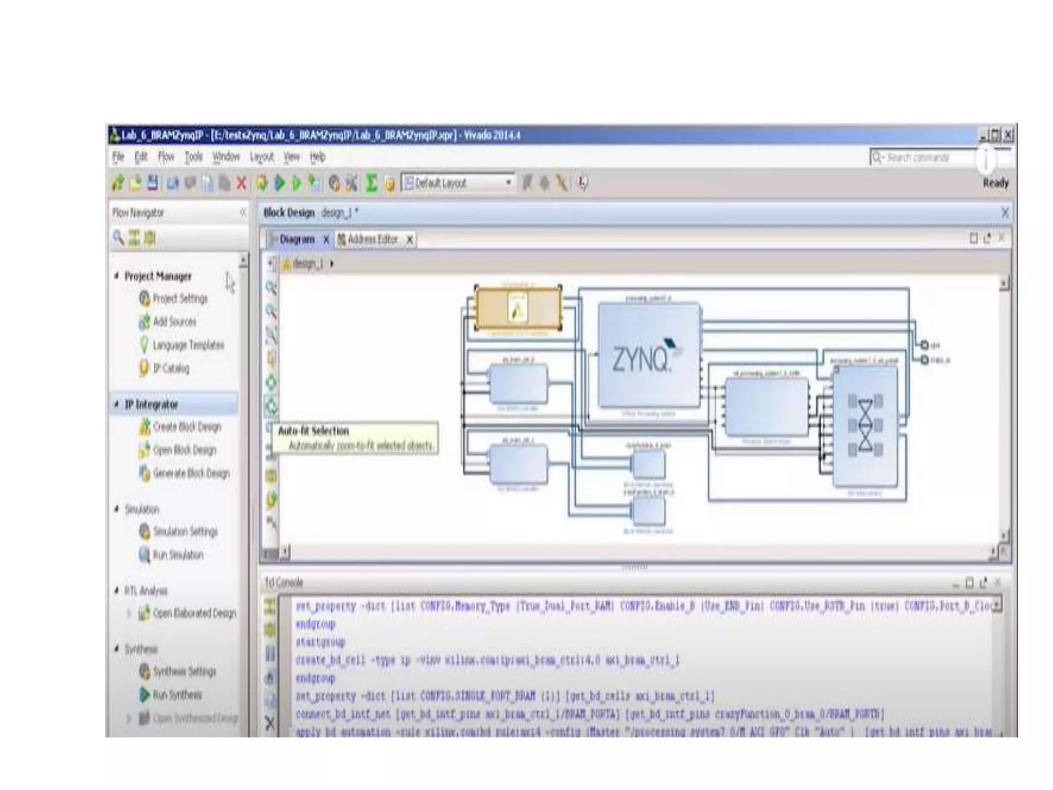
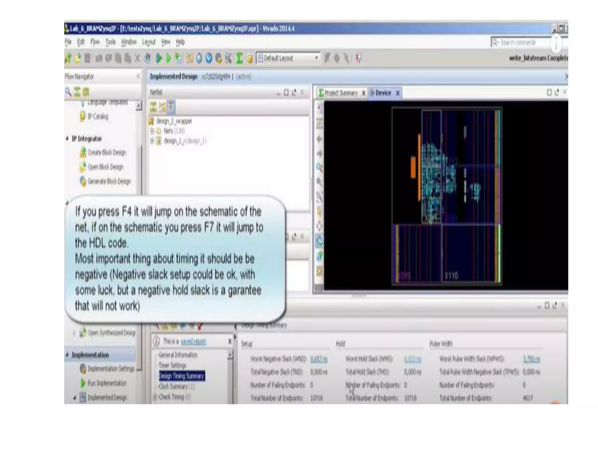
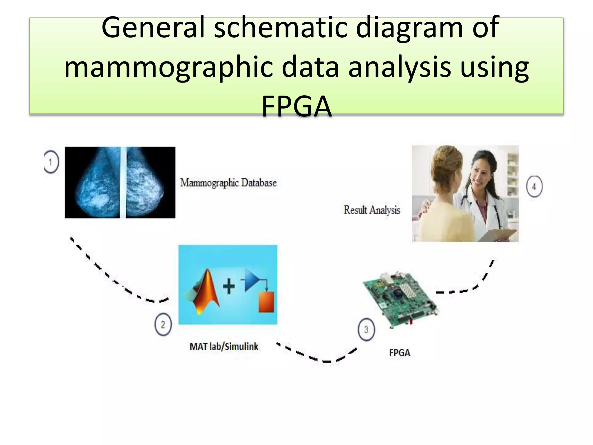
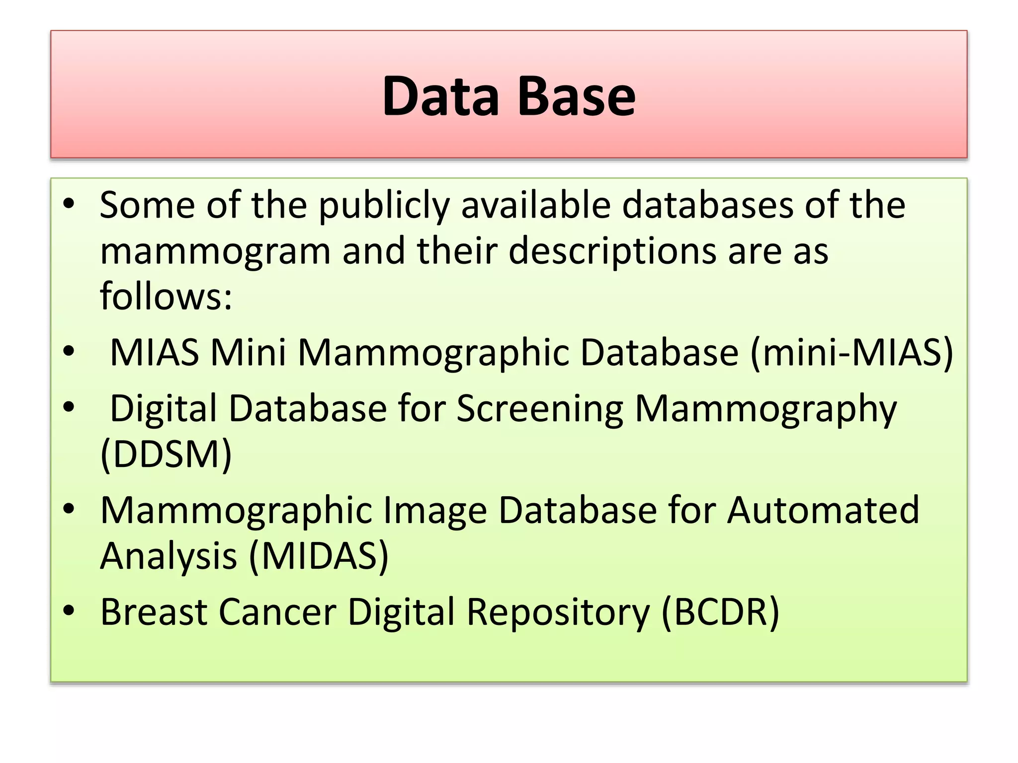
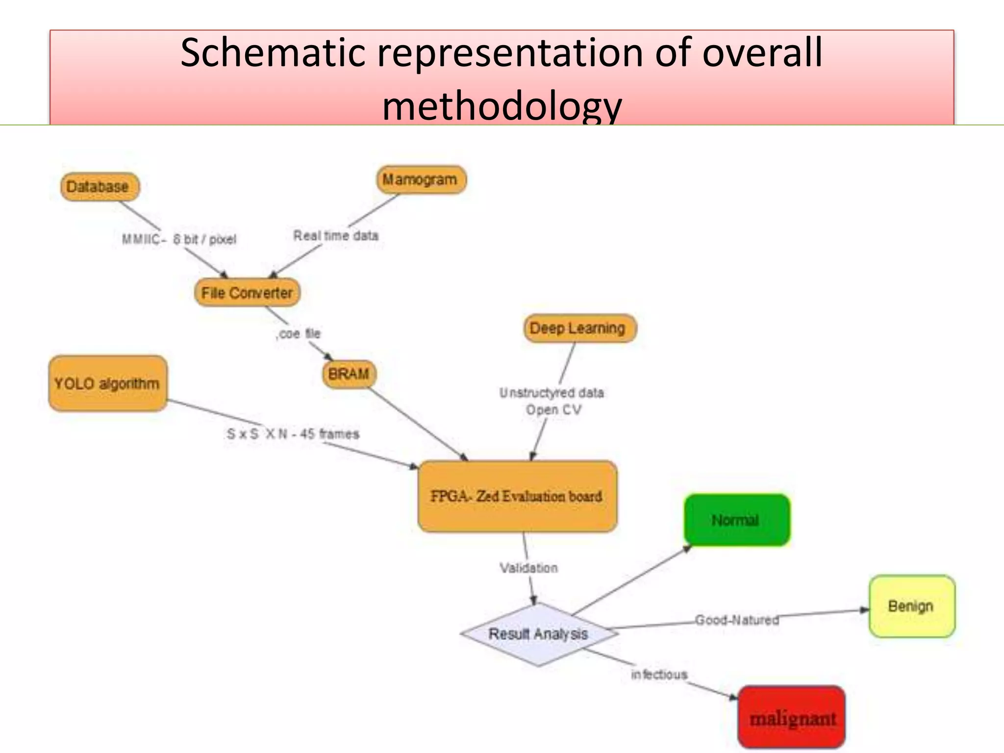
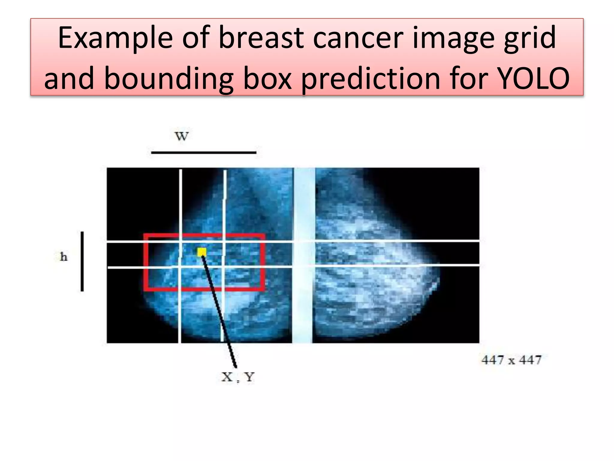
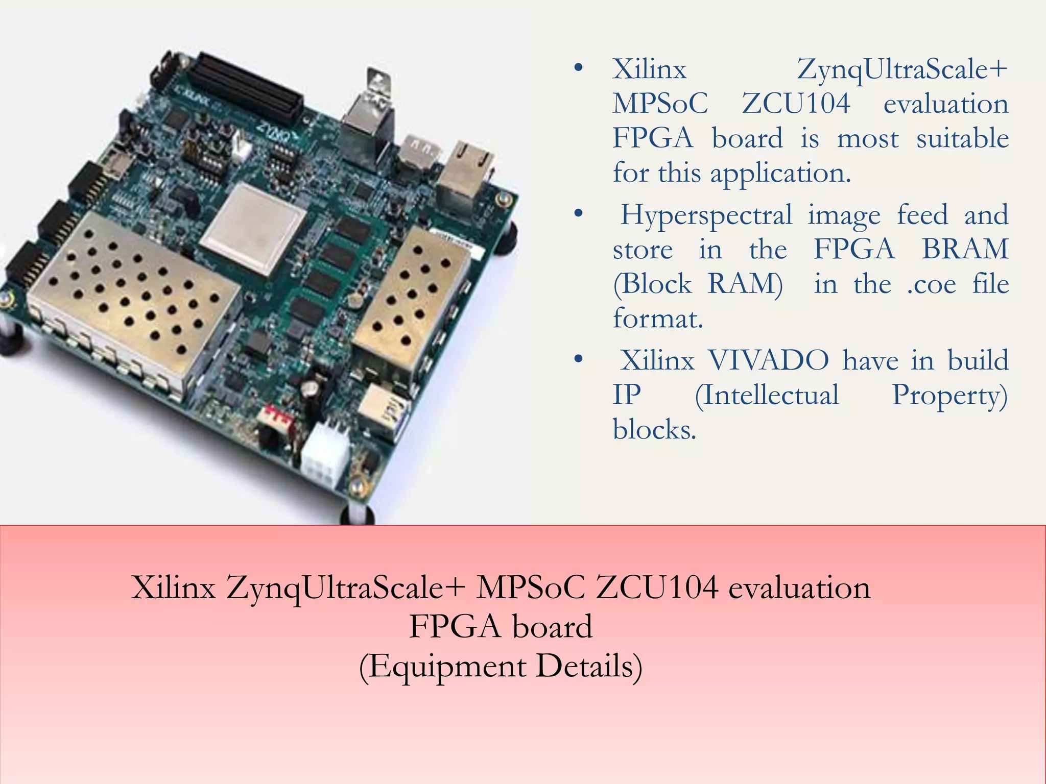
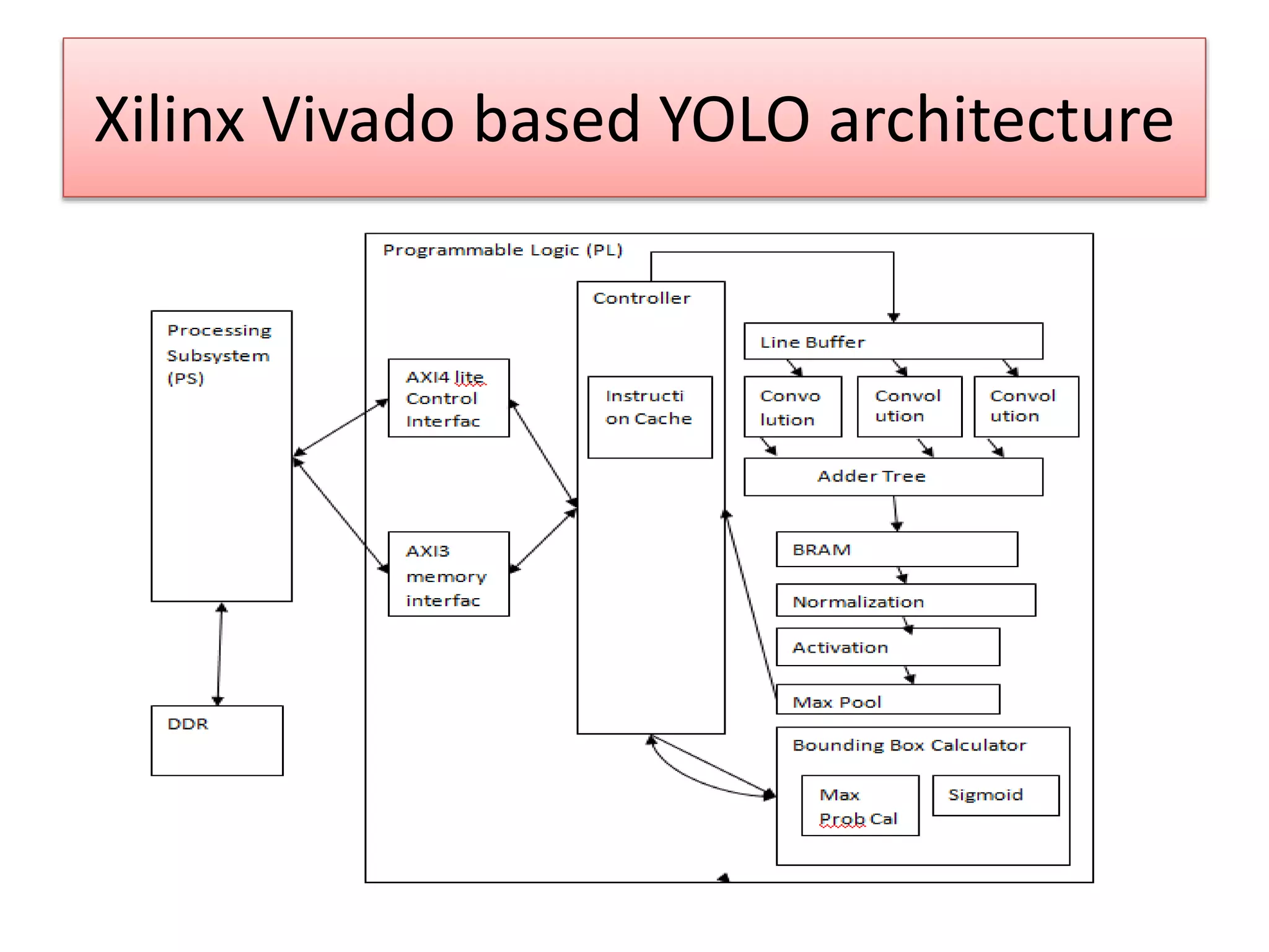
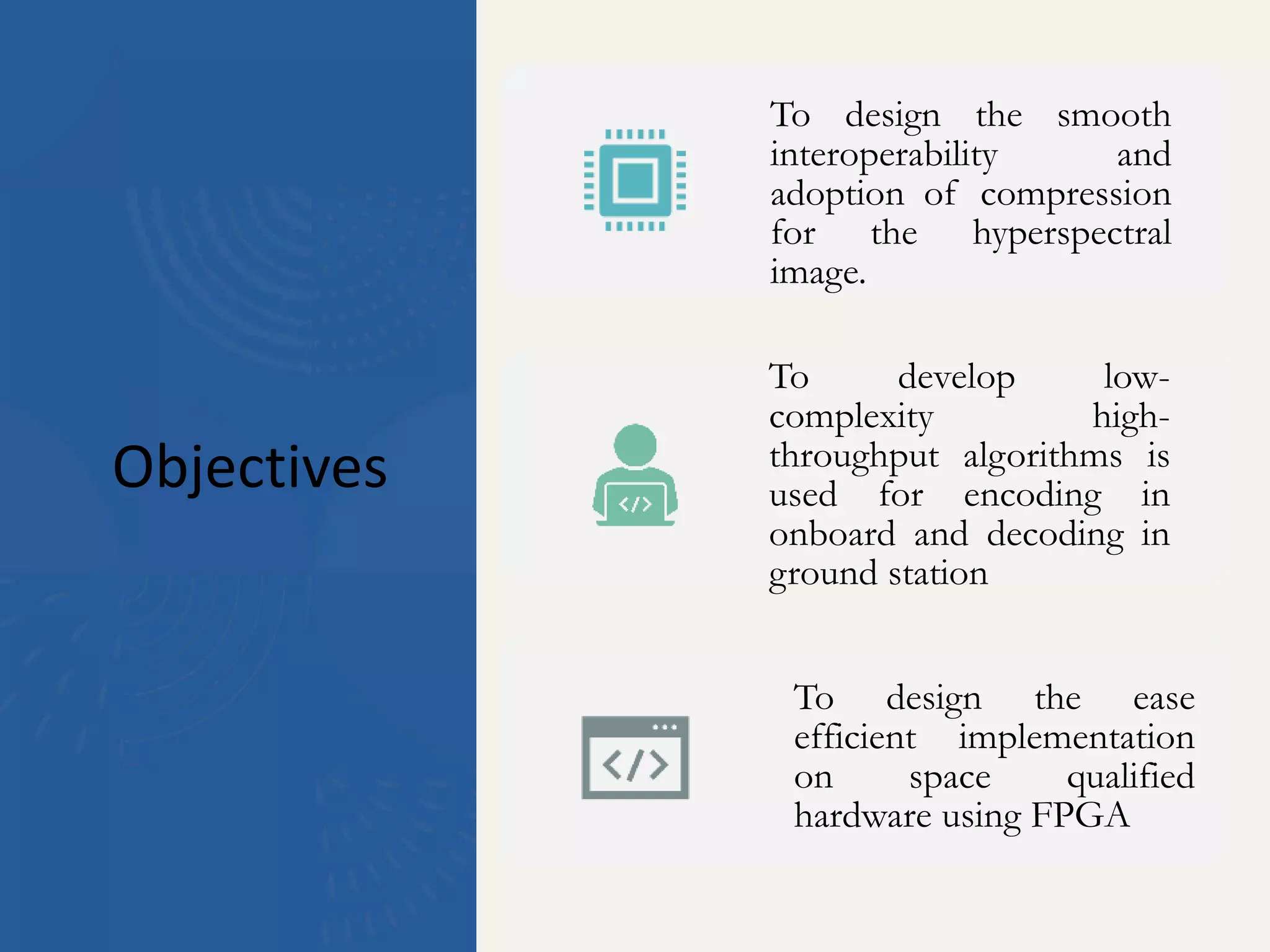
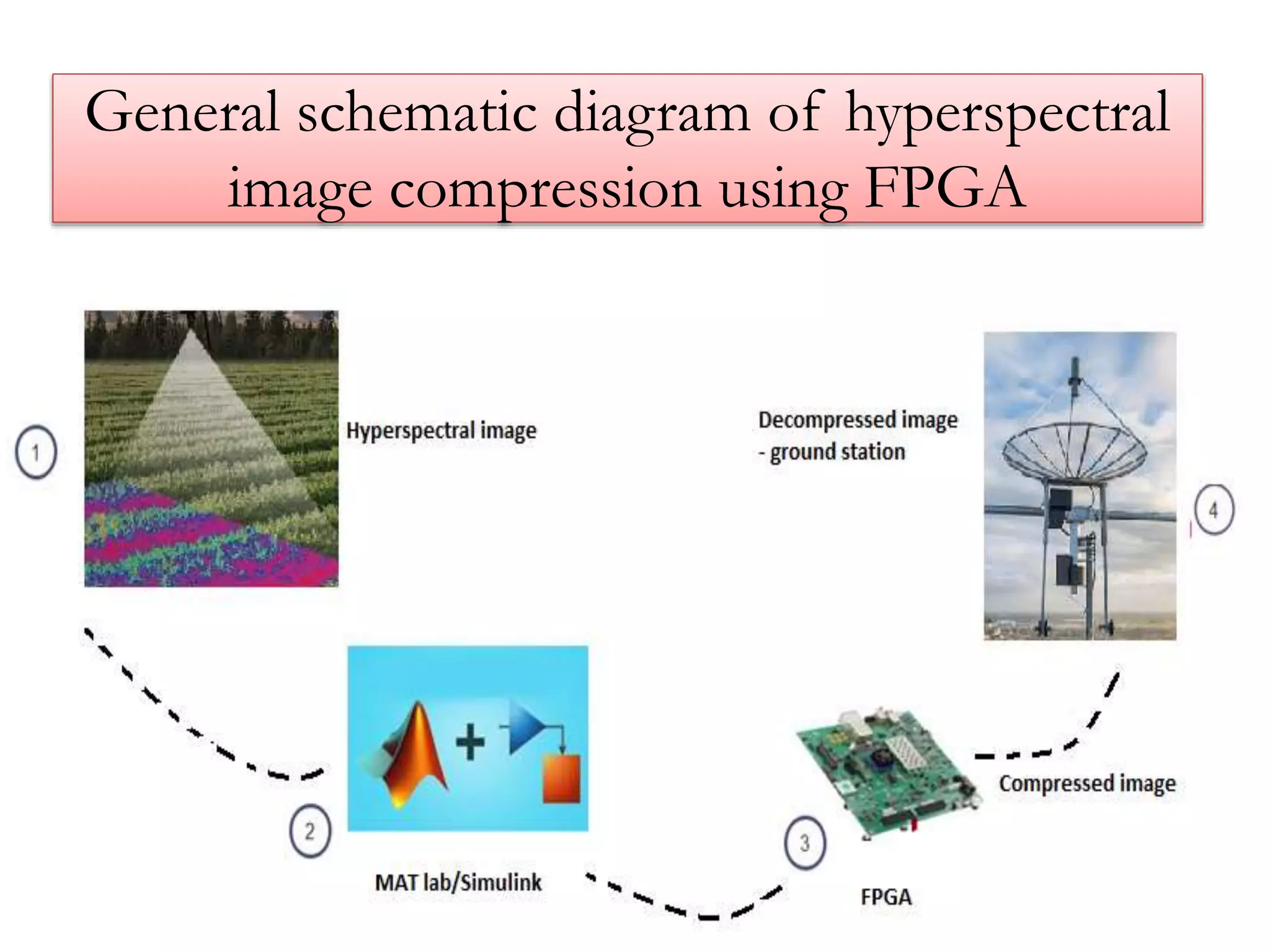
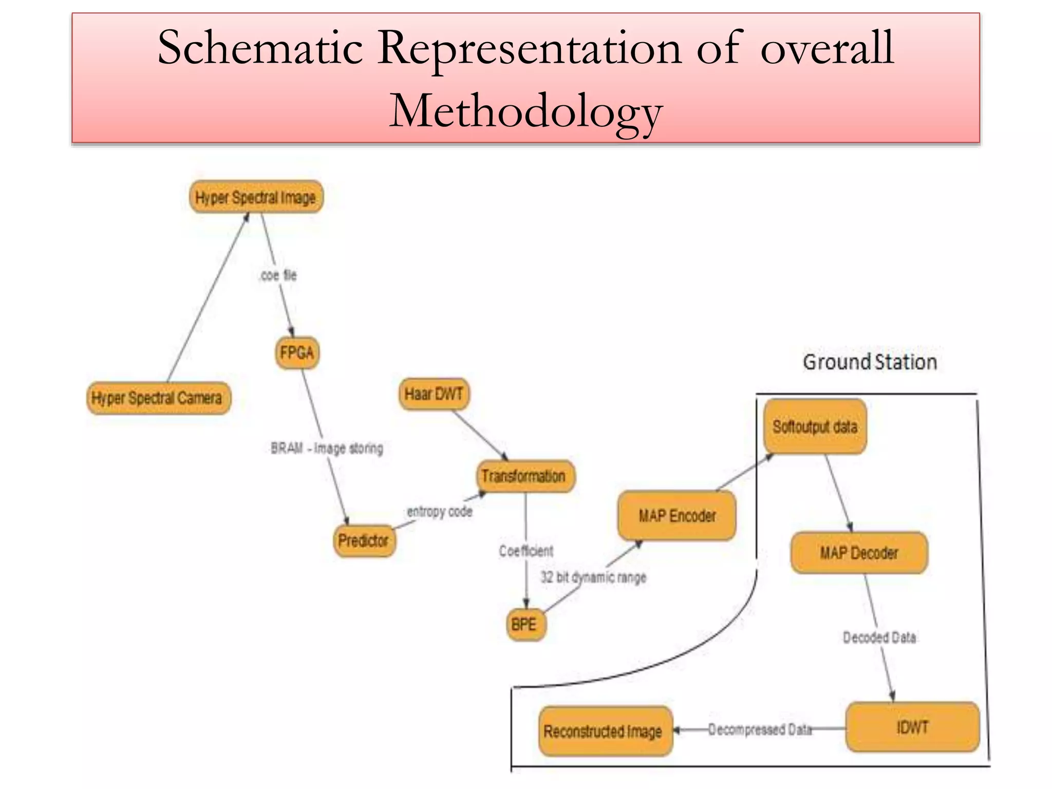
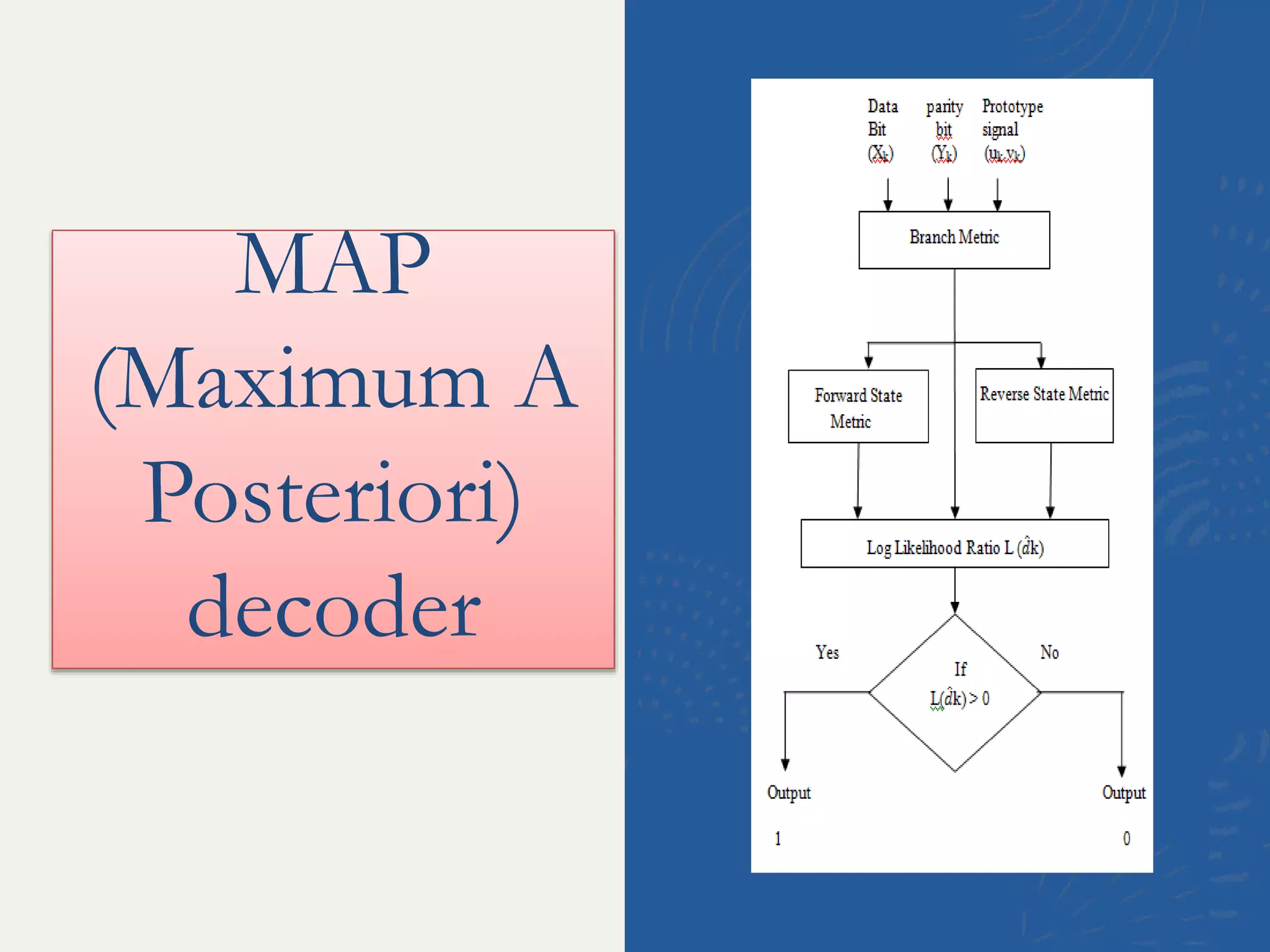
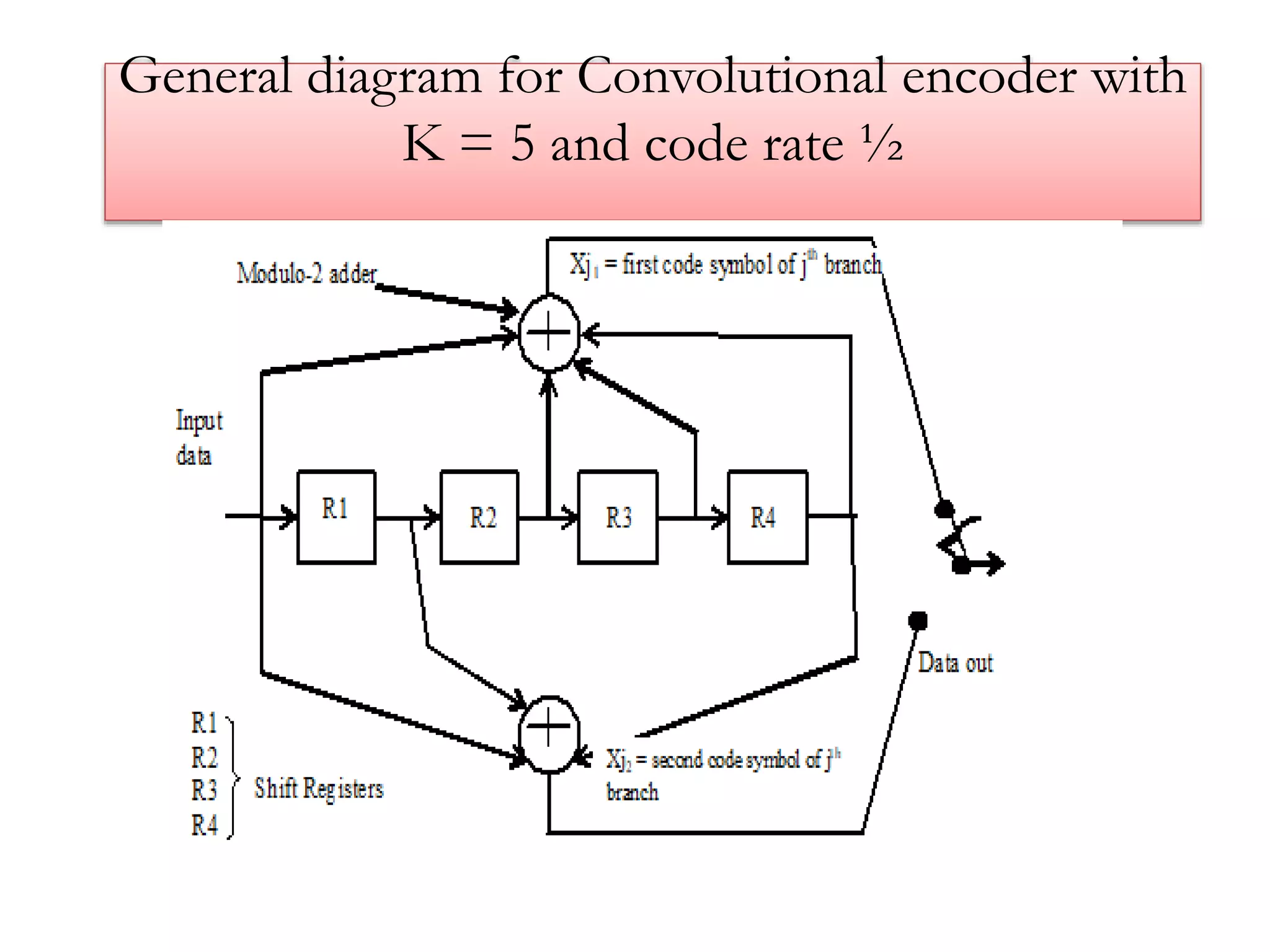
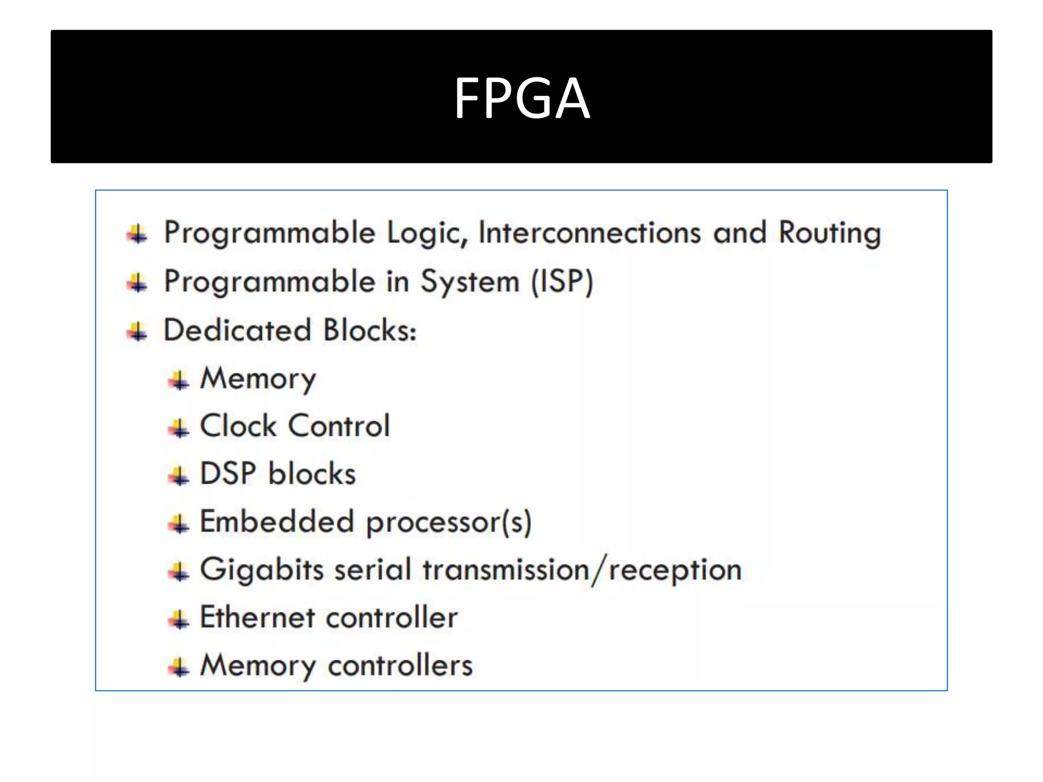
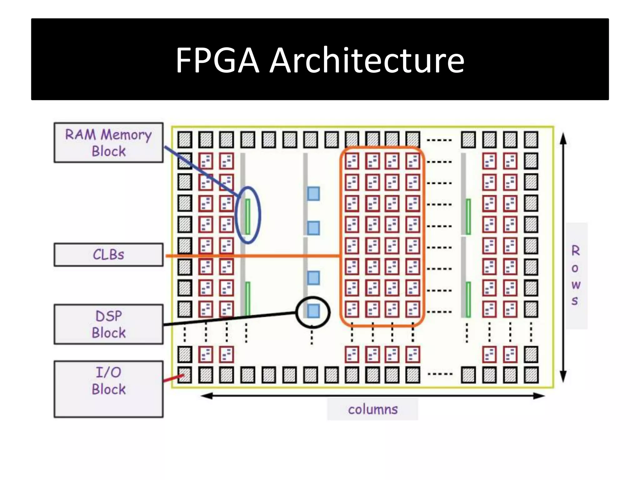
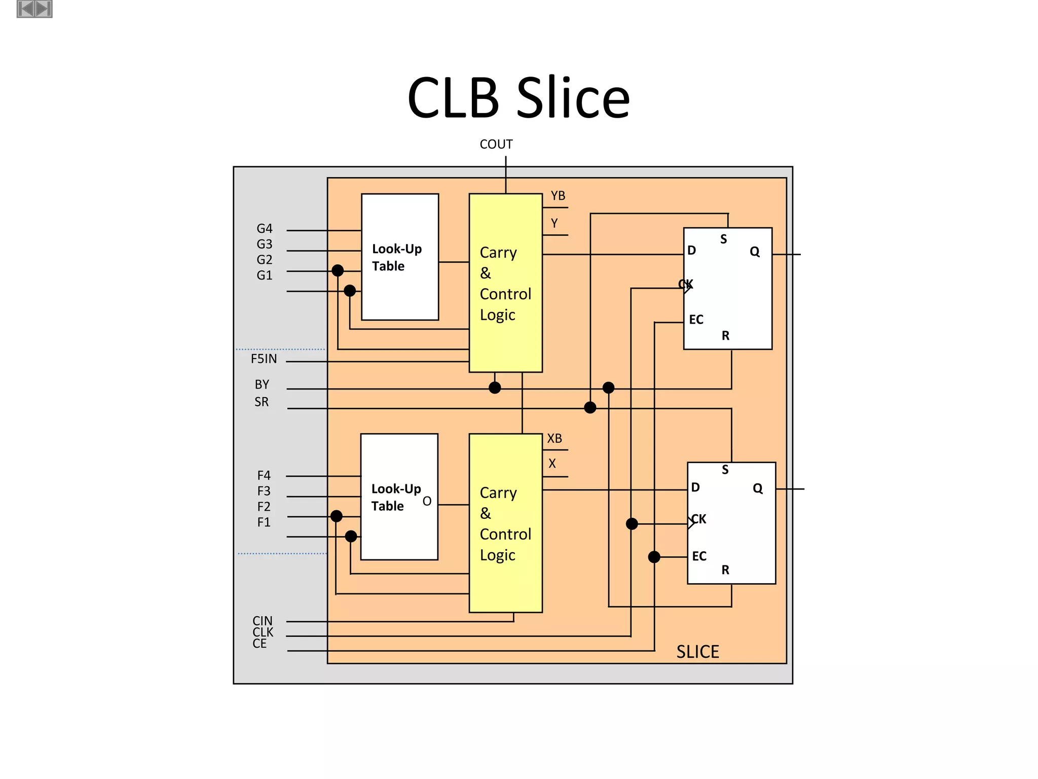
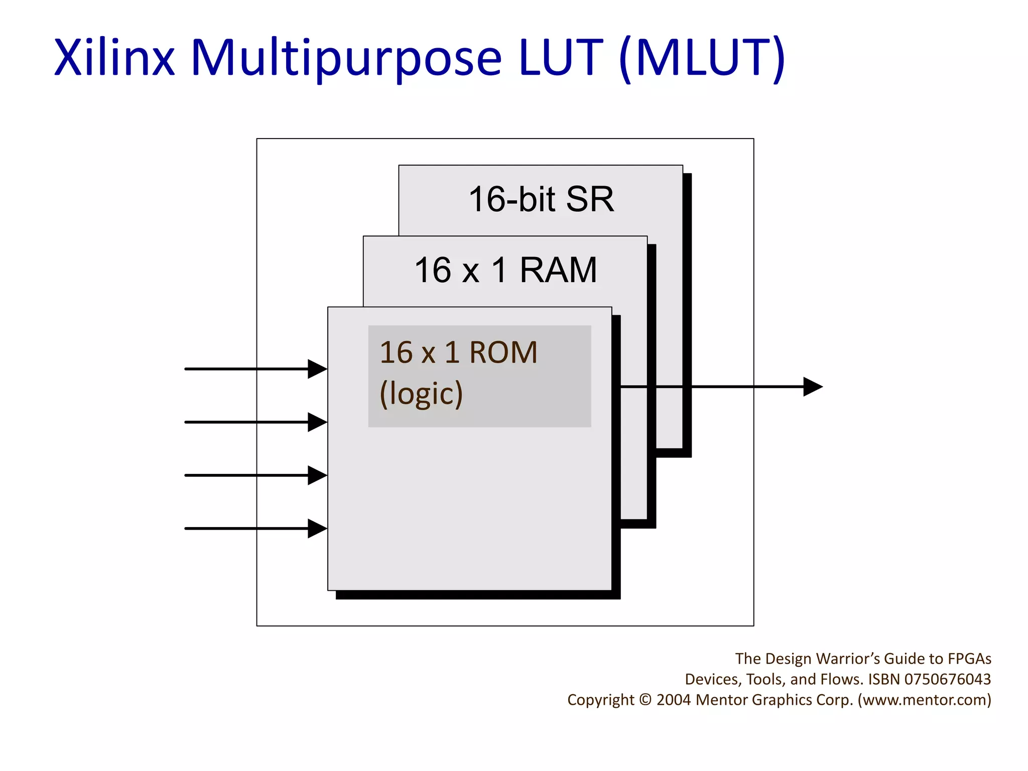
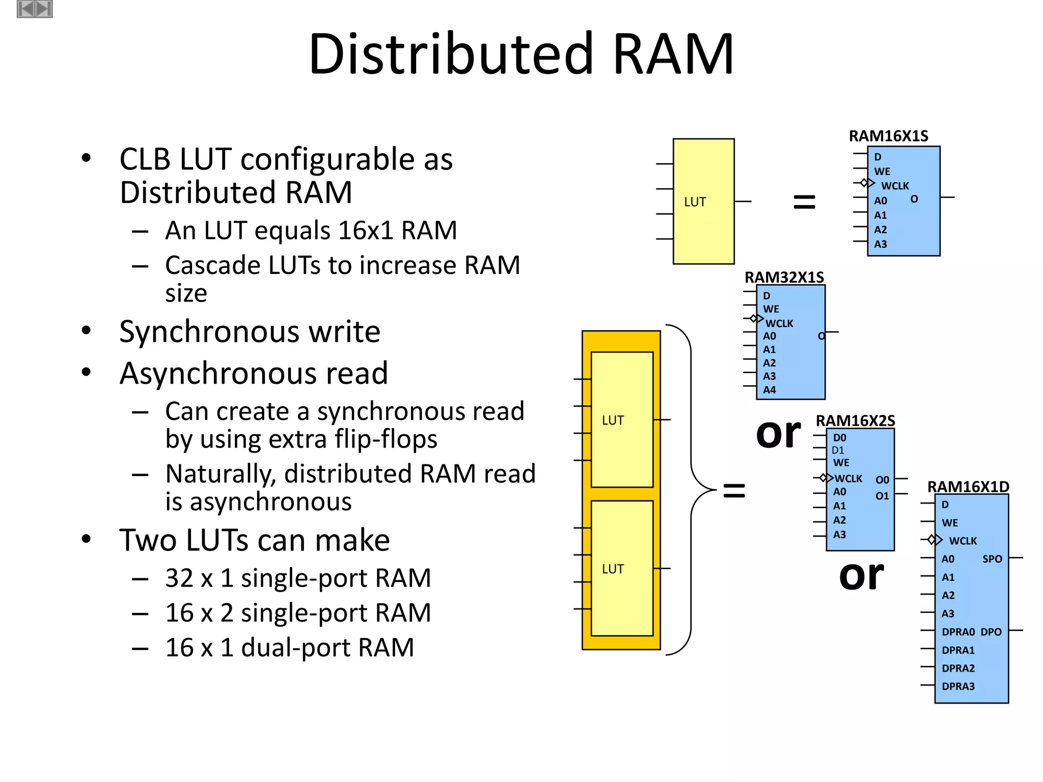
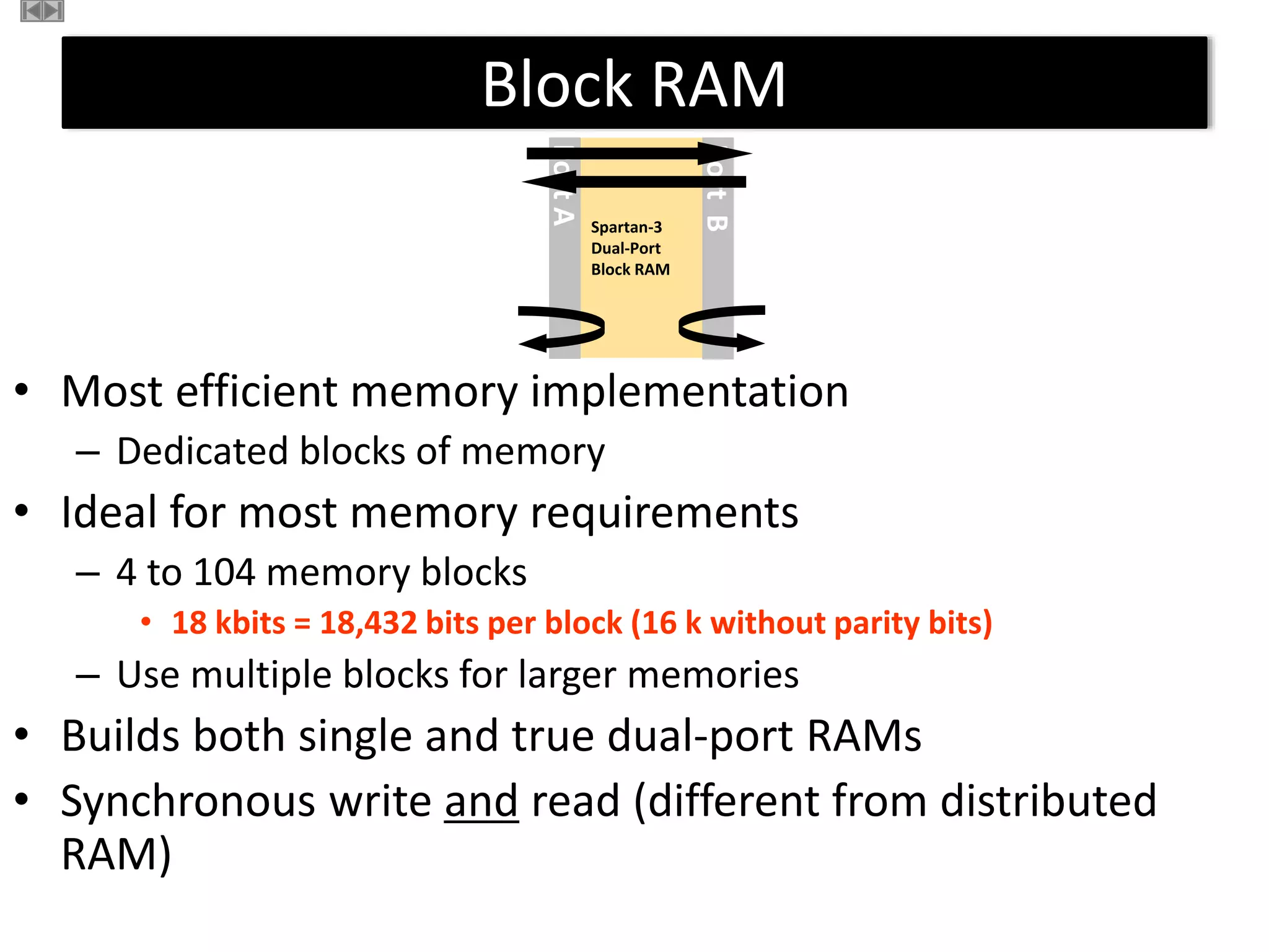
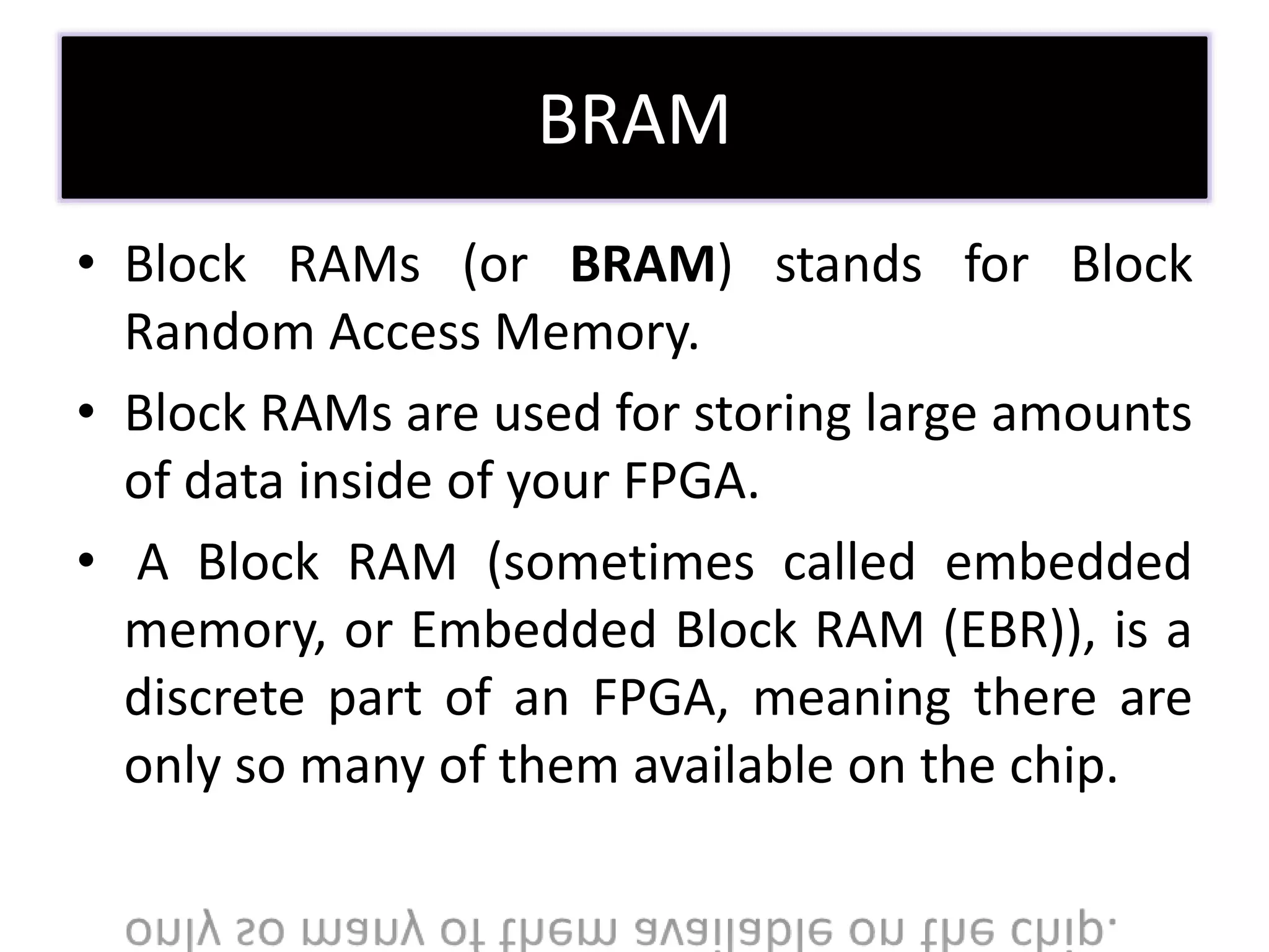
This document discusses image processing applications using Vivado for FPGAs. It provides information on FPGA architecture including distributed memory, block RAM features, and core generator. An example of a real-time breast cancer diagnosis application using YOLO on an FPGA board is described. A second example discusses implementing CCSDS standard DWT-based hyperspectral image decompression on an FPGA using techniques like Haar wavelet transform and MAP encoding.

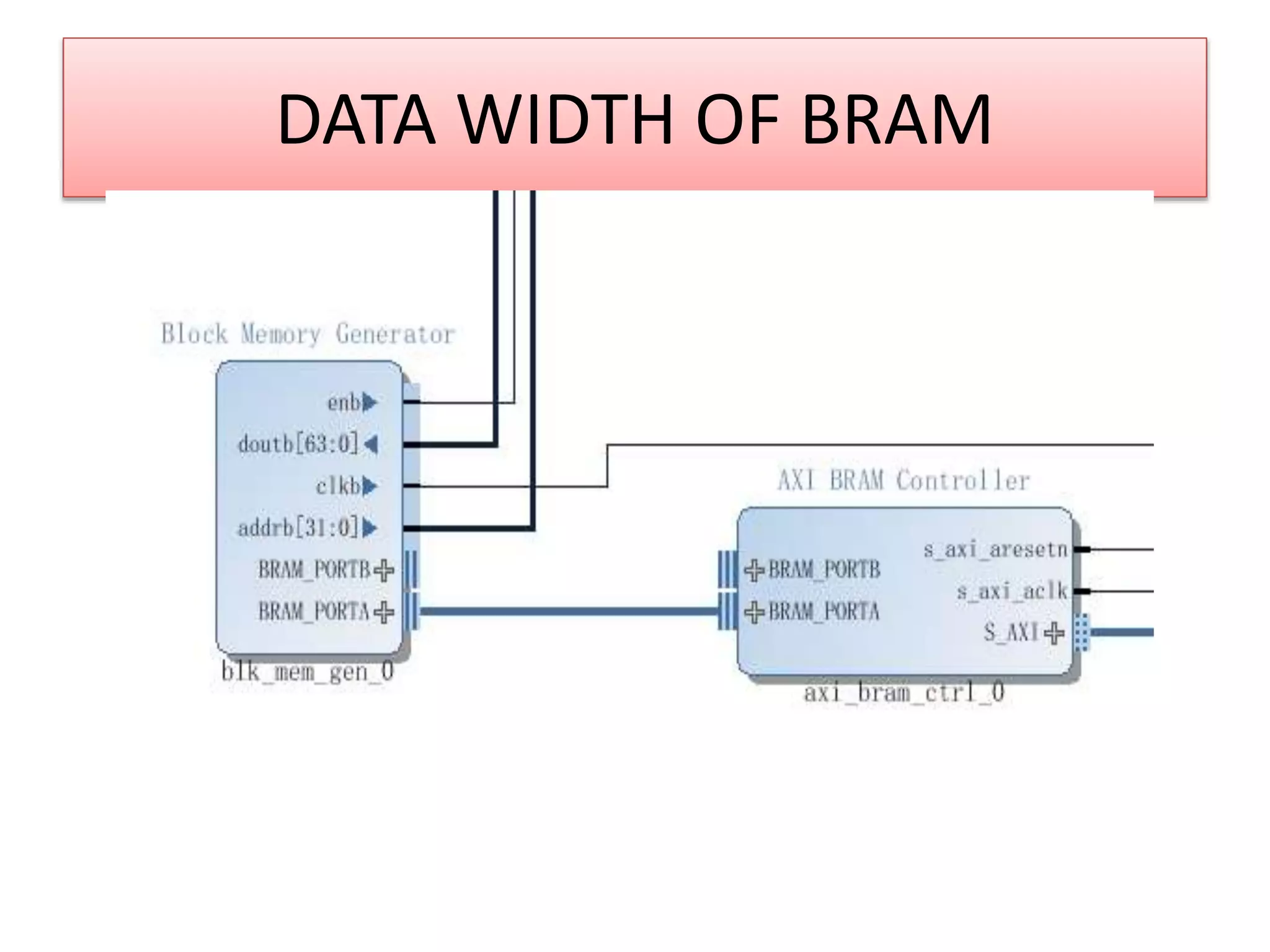
![BRAM Program sample
• module BMDEMO(
input clk,
input en,
input rst
);
wire [7:0]a,b;
wire [8:0]c;
reg [5:0]addr;
wire [8:0]bout;
blk_mem_gen_0 b1(clk,1'b0,addr,8'b1,a);
blk_mem_gen_0 b2(clk,1'b0,addr,8'b1,b);
adder a1 (a,b,c);
blk_mem_gen_1 b11(clk,1'b1,addr,c,bout);](https://image.slidesharecdn.com/dr-210731091345/75/Dr-s-shiyamala-fpga-ppt-20-2048.jpg)
![• always @(posedge clk or negedge rst)
begin
if(!rst)
addr = {{6'b1}};
else if(en)
addr=addr+1;
else
addr=addr;
end
endmodule
module adder(a,b,c);
input [7:0]a,b;
output [8:0] c;
assign c = (a+b);
endmodule](https://image.slidesharecdn.com/dr-210731091345/75/Dr-s-shiyamala-fpga-ppt-21-2048.jpg)