Download to read offline
![IJRET: International Journal of Research in Engineering and Technology ISSN: 2319-1163 | pISSN: 2321-7308
_______________________________________________________________________________________
Volume: 03 Issue: 07 | Jul-2014, Available @ http://www.ijret.org 394
Finally, we may conclude that based on the application
requirement bus protocols can be chosen. Even more types
bus protocols can also be implementing on FPGA and
compare with these bus protocols & even system can be
interfaced to PC through USB interface.
REFERENCES
[1]. S.Thane, S.Somkuamanit, S.Khuntawee.
“Implementation of Multi-Protocol, Data Acquisition with
High Speed USB interface, Using FPGA”, The International
Multi Conference of Engineers and Computer Scientists
(IMECS)- Vol I, March 17-19, 2010. Hong Kong.
[2]. Frédéric Leens, “An Introduction to I2C and SPI
protocols”. IEEE Instrumentation & Measurement Magazine
February 2009.
[3]. Bollam Eswari, N.Onmagal, K.Preethi, S.G. Sreejeesh,
“Implementation of I2C Master Bus Controller on FPGA”.
International Conference on Communication and Signal
Processing, April 3-5, 2013, India.
[4]. Bernhard Linke, “Overview of 1-Wire Technology and
Its Use”, Jun 19, 2008, Maxim Integrated Products, Inc.
[5]. Volnei A.Pedroni, “Circuit Design with VHDL”,MIT
Press, England.
[6]. Douglas L. Perry, “VHDL: Programming by Example”
4th
Edition.
BIOGRAPHIES
Chetan Umadi completed his Bachelor of
Engineering at K.L.S Vishwanath Rao
Deshpande Rural Institute of Technology,
Haliyal. Karnataka India in 2012.He is
Pursuing Master in Technology at
Dr.Ambedkar Institute of Technology,
Bangalore, India. His areas of interest are Digital design and
Embedded System Design.
Dr. G.V. Jayaramaiah completed his
Ph.D. From IIT-Bombay. He has
published around 19 Papers in
international journals. He is working as
Professor and Head of the department of
ECE at Dr.Ambedkar Institute of
Technology. Bangalore. India. His areas of interest are
Power Electronics, Renewable Energy and Embedded
Systems.](https://image.slidesharecdn.com/fpgaimplementationofmulti-protocoldata-140821043823-phpapp01/85/Fpga-implementation-of-multi-protocol-data-5-320.jpg)

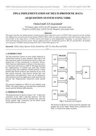
This paper presents the FPGA implementation of a multi-protocol data acquisition system using VHDL, which supports four different bus protocols: parallel, SPI, I2C, and one-wire. The system is designed to acquire data from multichannel sensors and transmit it effectively, with simulations demonstrating the performance and comparison of each protocol. Conclusions highlight the choice of bus protocols based on specific application requirements, emphasizing the trade-offs between speed, pin count, and functionality.