Downloaded 12 times

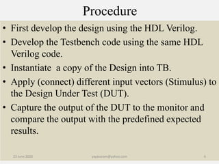


![Ex:Up Counter
module up_count (output reg[7:0] out,
input wire enable , input wire clk , input wire rst);
always @(posedge clk) //behavioural model
if (rst)
begin
out <= 8'b0;
end
else if (enable)
begin
out <= out+1;
end
endmodule](https://image.slidesharecdn.com/verilogtestbench-200712173255/85/Verilog-Test-Bench-14-320.jpg)
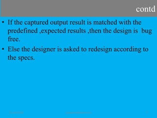
![Up-Counter-TB
• module test_upcount;
wire [7:0]out;
reg enable, clk, rst;
upcount uut(out,enable,clk,rst); // Module Instantiation
initial begin
clk = 0;
rst = 1;
enable = 0; #20;
end
23 June 2020 yayavaram@yahoo.com 15](https://image.slidesharecdn.com/verilogtestbench-200712173255/85/Verilog-Test-Bench-15-320.jpg)


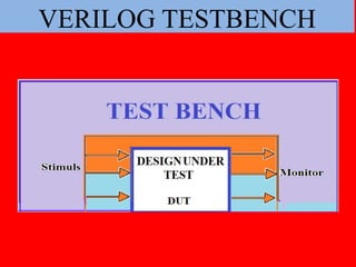
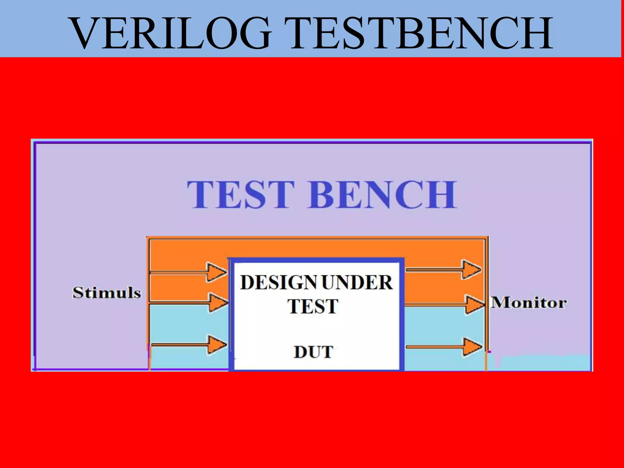
The document discusses the process of verifying a chip's design using a Verilog testbench, which is a HDL code that applies input stimuli to the design under test (DUT) and captures its output for comparison with expected results. It outlines the structure and steps for creating a testbench, including initializing inputs, generating test vectors, and checking the DUT's behavior against predefined outputs. The document also provides examples of testbenches for various digital circuits, such as NAND gates, half-adders, and full-adders.