Downloaded 18 times


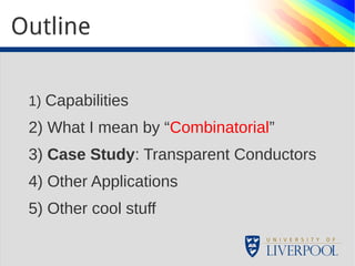

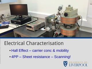

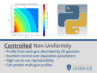
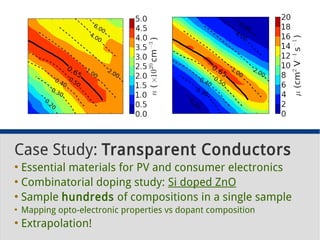
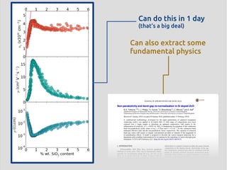
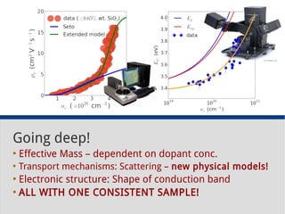
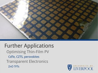
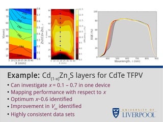
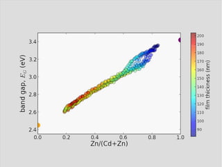


The document discusses rapid optimization techniques for thin-film materials and devices, highlighting capabilities such as controlled non-uniform deposition and advanced characterization methods. A case study on transparent conductors is presented, illustrating the benefits of combinatorial doping studies for efficient material mapping and performance optimization. Further applications and breakthroughs in thin-film photovoltaics and transparent electronics are also mentioned, along with new developments in perovskite films.


