Download to read offline
![Effective testing for wafer reject minimization
by terahertz analysis and sub-surface imaging
Anis Rahman and Aunik K. Rahman
Applied Research & Photonics
470 Friendship Road, Suite 10
Harrisburg, PA 17111, USA
a.rahman@arphotonics.net
Abstract— This paper outlines applications of terahertz
spectrometry, terahertz reflectometry and sub-surface imaging
for effective characterization of various aspects of semiconductor
wafer testing. Exemplary results of scanning a wafer have been
analyzed for defect determination. Additionally, terahertz
reflectometry for controlling wafer polishing for planarization
has been exemplified via high precision thickness monitoring.
Application of terahertz spectrometry for identifying self-
assembled monolayer (SAM) on a wafer is also outlined with
example. The technique may be extended to other substrates
transparent to terahertz radiation. Characterizing different SAM
coated silicon wafers for identifying two different SAM species
has been discussed. The Fourier transform absorbance spectra
of both SAM specimens reveals several distinguishable
absorbance peaks that may be used as signatures of the
respective SAMs. The SAM having 18 carbon chain exhibits
higher absorbance than that of the SAM comprised of 8 carbon
chain. This is consistent with the higher molecular weight of the
former.
Keywords—Terahertz spectrometry; Terahertz reflectometry;
Terahertz scanner; sub-surface imaging; wafer defect analysis;
Wafer thickness monitoring; Self-assembled monolayer on wafer
I. INTRODUCTION
Terahertz spectrometry [1] and reflectometry [2] offers an
effective solution for wafer reject minimization by means of
sub-surface, nano scale, 3D imaging, via a non-destructive and
non-contact route. A terahertz sub-surface 3D imager (Applied
Research & Photonics) has been used for the current
investigations. Simultaneous reflection and transmission
measurements allow inspection of semiconductor wafers
during fab processes (in-situ) as well as for post-fab characteri-
zations (ex-situ). The intensity of the reflected terahertz beam
is proportional to the specific features (layers) of the specimen
under test. Therefore, measured intensity may be modeled in
terms of suitable physical parameters such as refractive index,
density, dielectric constant, etc., via a modified Beer-Lambert’s
law. For a given wafer, all material parameters remain
unchanged during measurements, because, terahertz radiation
is non-ionizing and does not perturb the intrinsic properties.
Thus, the reflectance, is proportional to the variations in
materials at the point where the beam is incident. As such, the
reflectance is dependent on the spatial and angular coordinates:
( ) A 3D reconstructed image generated from
reflectance, therefore, will yield the characteristic features
(patterns) on the substrate. Another advantage of the terahertz
scanner is that silicon and other semiconductor wafers are
transparent at these wavelengths. Therefore, scanning may be
done across the thickness of a wafer for inspecting internal
layers. So, if there is a hole or void on the substrate or in any of
the sub-surface layers, that will be identifiable from both
reflected and transmitted intensities. Based on the above
principle, a signature of a given defect may be established. Any
defect such as, inclusions, cracks, non-uniformity, or
particulate foreign material can be detected and identified by
this technique. Moreover, defect size may be estimated from
either a 2-D scan, or 3-D scanned reconstructed imaging. The
terahertz nano-scanner deploys a non-contact measurement
system with an adjustable stand-off distance. The sample space
is adjustable to accommodate required sample size. A rotary
axis enables examination of a wafer (or other sample) from
different viewing angles. This is important because cracks or
other non-uniformities might not be along a straight line-of-
sight. Thus an angular scan enables viewing hidden features. In
addition, with the advent of the angular axis, one can scan
cylindrical objects in a conformal fashion.
Another important issue for the semiconductor wafers is the
requirement of planarization as the fabrication process
progresses with layer by layer deposition and patterning.
Chemical and mechanical polishing (CMP) used for wafer
planarization requires just sufficient material to be removed,
but too much removal can result in failure/rejection of the
wafer. As such precise thickness control, on the order of
nanometers, is required for lowering the reject rate. Terahertz
transmission and/or reflection measurements can be used for
monitoring the CMP process. Here, we report a technique for
controlling the polishing process based on given thickness
criterion. The removal of material from the wafer surface is a
complex function of the polishing slurry, spin speed and
duration, among other factors. However, a straightforward](https://image.slidesharecdn.com/asmc20145-140523182705-phpapp01/85/Asmc2014-5-8-1-320.jpg)
![method that minimizes monitoring of individual variables is
the direct measurement of the thickness of the wafer, from
which the mass of the removed material may also be
calculated. In this technique a terahertz beam is reflected off of
the polishing surface while a transmission measurement may
also be carried out simultaneously. A requirement of this
technique is a rigorous calibration of the material removal as a
function of polishing conditions while all physical parameters
essentially remain fixed. This process reduces the number of
control variables to a single parameter, i.e., reflected (and/or
transmitted) power vs. thickness removed.
Additionally, semiconductor wafers’ surface needs to be
modified for different chemistry in preparation of processes
such as patterning of waveguides or CMOS process with
different functionalities. Common surface modification
involves making a wafer hydrophilic or if it is already
hydrophilic then converting it to hydrophobic. This is uniquely
done by various self-assembled monolayers (SAMs). However,
it is difficult to characterize the SAMs with common laboratory
instruments (e.g., UV/Vis, Raman or FTIR), because, SAMs
being only one molecule thick layer, physical characterization
between different SAMs applied on wafer surfaces is
challenging. Terahertz spectroscopy offers an advent of
characterizing the molecular systems – even with minimal
structural and mass differences – owing to its ultra-high
sensitivity stemmed from the fact that terahertz photons
interact with the entire molecule as opposed to a bond or a
charge states as used by its predecessors.
In the followings, exemplary results of wafer scans have
been analyzed for defect determination. Additionally, terahertz
reflectometry for wafer polishing has been exemplified with
data. Finally, application of terahertz spectrometry for
identifying self-assembled monolayer (SAM) on a wafer is also
outlined with example.
II. EXPERIMENTAL
Fig. 1 displays a schematic diagram of the terahertz nano-
scanner. Here the wafer is mounted on a rotary stage which is
mounted on a XYZ stage. The measurement system comprises
of an electro-optic dendrimer based continuous wave (CW)
terahertz source and a matching detection system that was
described elsewhere [3]. All positioning stages are automated;
the linear stages have a resolution of ~25 nm. As shown in Fig.
1, this design is based on normal incidence of the terahertz
beam to the target. In case of normal incidence, the incident
beam is the sum of the reflected, transmitted, absorbed and
scattered intensities. Assuming the material properties remain
unchanged during measurement, the reflectance will be
proportional to the material characteristics. Ordinarily, the
Beer-Lambert’s law is used to determine the concentration, C,
of a solute in a solvent from absorbance data: A= εlC, where l
is the path length and is the extinction coefficient (or molar
absorptivity). Since the reflectance, R, is material dependent, a
modified Beer-Lambert’s law may be stated as,
( ) ( ) ( ) ( ), (1)
where, the reflectance is coordinate dependent because the
materials on a wafer is position dependent, which in turn
causes variation in the path length, ( ), and consequently
variation in the coefficient ( ) . It is notable that, the
coefficient ( ) may be used for modeling desired material
parameters such as density, dielectric constant, refractive
index, etc. Obviously, this modeling gives the effective value
of the chosen parameter as opposed to the complex quantity.
Mapping of R(r) yields a 3D visualization of the specimen. Fig.
2 shows a 3D surface plot of a wafer where different features
are depicted by different colors and their sizes are as indicated
by the coordinates of the axes.
III. RESULTS AND DISCUSSION
A. Wafer inspection
Fig. 3 shows a pattern of adjacent dies on a wafer revealed
by a 1D scan. Fig. 3 also shows that adjacent layers are
detectable by their unique reflected intensity. A high resolution
scan thus clearly shows the start, the end, and intricate pattern
for each die on a wafer (Fig. 3 lower plot). The repetitive
pattern from high resolution scan serves as a distinguishing
Figure 1. Schematic representation of the nano-scanner.
Fig. 2. A 3D image of a wafer area.](https://image.slidesharecdn.com/asmc20145-140523182705-phpapp01/85/Asmc2014-5-8-2-320.jpg)
![metric for good dies from the bad ones. Since the scans are in
exact coordinates, one can inspect the patterns closely for their
irregularity and/or defect conditions. Once a defect position is
identified, insight from process parameters may be used to
Fig. 3. High resolution scan pattern from two different segments of a
wafer. Both top and bottom segment clearly show the start, end,
and intricate pattern for each die.
Fig. 4. Reproducibility of the traces. Slight mismatch is due to the
course resolution of the stage.
deduce the actual nature of the defect. Fig. 4 shows the
reproducibility of the measurements. Fig. 5 shows a
reconstructed sub-surface image of an area; a comparison of
such images between a good and a bad area will reveal the
exact position and layer of the defect.
Fig. 5. Reconstructed 3D representation of problem area. A series of
1-D scan in the X-direction was made at different heights to
reconstruct the 3-D profile. Some small features are visible.
B. Wafer polishing
In order to demonstrate the resolution of mass removal of a
silicon wafer by polishing, a piece of Si-wafer was gradually
polished by hand on an 800-grit sand paper. The wafer was
weighed after each polish by a lab microbalance, mounted on
the THz spectrometer (Fig. 6) and transmitted power (in
counts) vs. the removed mass was recorded. Fig. 7 shows that
as the mass is removed by polishing, the transmitted power
increases successively for each polish, indicating that
transmitted power is an inverse function of removed mass.
The results were used for computing the corresponding
thickness from known area and density of the wafer. Fig. 8
shows the computed thickness vs. the change in measured
power. The slope of Fig. 8 indicates that for each nanometer
thickness removed, the counts difference is 8.15 million. The
noise floor of the detection system is ~ ± 5103
counts. Thus,
the uncertainly in the thickness data of Fig. 8 is < ± 10 pm.
Therefore, it is demonstrated that THz transmission
measurement can be used for high precision thickness
monitoring of wafer’s planarization process. Thus, a control
system operated by this monitoring system is expected to
maintain high level of uniformity of the CMP process.
However, the actual CMP process involves use of polishing
slurry and other chemicals. Therefore, the performance of this
system must be determined via calibration for an actual CMP
system. In addition, different calibration will be necessary for
different slurry and polishing protocol combinations.
C. Self-assembled monolayers on wafer
Self-assembled monolayers (SAMs) were fabricated on
double side polished silicon wafers [4]. Two different SAMs
have been used. (1): n-Octadecyltrichlorosilane (abbreviated
as C-18), Mw = 387.93 g/mol; and (2): 7-OCT-1-
Enyltrichlorosilane (abbreviated as C-8); Mw = 245.65 g/mol.
The experimental setup was described elsewhere [1]. As
received SAM coated wafers were mounted on the
spectrometer with similar arrangement as shown in Fig. 6.
Terahertz time-domain spectra were acquired with the
TeraSpectra front end [5]. Fig. 9 shows the comparison of
time-domain signals of the two samples. The SAM C-8,
having lower number of carbons, exhibit higher transmission](https://image.slidesharecdn.com/asmc20145-140523182705-phpapp01/85/Asmc2014-5-8-3-320.jpg)
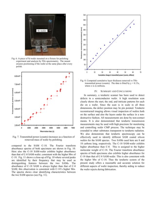
![Fig. 9. Temporal signal of silicon wafer coated with two different
SAM. C8 having 8 carbon chain has a higher transmission
compared to C18, an 18 carbon chain molecule.
Fig. 10. The absorbance spectra of two SAMs on silicon wafer.
Several peaks may be identified for characteristic differences
between the two SAM species.
REFERENCES
[1] Rahman, Anis., Dendrimer Based Terahertz Time-Domain Spectroscopy
and Applications in Molecular Characterization. Journal of Molecular
Structure, 2011. 1006: p. 59-65.
[2] A. Rahman, S. Frenchek, B. Kilfoyle, L. Patterkine, A. K. Rahman, and
B. Michiniak-Kohn, “Diffusion kinetics and permeation concentration of
human stratum corneum,” Drug Development & Delivery, May 2012,
pp. 43–49.
[3] A. Rahman and A. K. Rahman, “Wide Range Broadband Terahertz
Emission From High (2) Dendrimer,” in Terahertz Technology and
Applications V, edited by Laurence P. Sadwick, Créidhe M. O'Sullivan,
Proc. SPIE Vol. 8261, 82610H (2012).
[4] “Investigation of self-assembled monolayers on silicon wafer by
terahertz spectrometry,” white paper:
http://arphotonics.net/THzSpectraSAMonSiliconWafer.pdf.
[5] http://arphotonics.net/TeraSpectraBrochure_spec_2011_.pdf
Fig. 11. The absorbance spectra of both SAMs (same as Fig. 10,
but X-axis truncated to 20 THz). Several peaks may be
identified for characteristic differences between the two
SAM species.](https://image.slidesharecdn.com/asmc20145-140523182705-phpapp01/85/Asmc2014-5-8-5-320.jpg)

1) The document outlines applications of terahertz spectrometry, reflectometry, and sub-surface imaging for semiconductor wafer testing to minimize wafer rejects. 2) Exemplary results are analyzed from scanning a wafer to determine defects. Terahertz reflectometry is also shown to effectively control wafer polishing by precisely monitoring thickness. 3) The technique can also identify different self-assembled monolayer coatings on wafers by analyzing their terahertz absorption spectra signatures.


![5G Explained! A High Level Overview [Introduction]](https://cdn.slidesharecdn.com/ss_thumbnails/5gexplainedahighleveloverview-260119165306-cc137a3e-thumbnail.jpg?width=640&height=640&fit=bounds)


