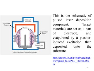
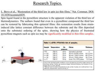
Downloaded 46 times
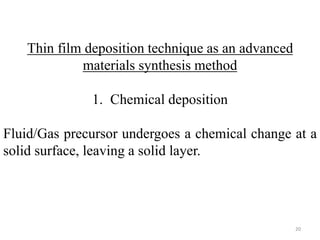
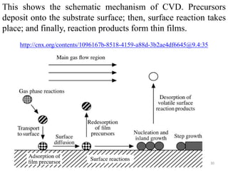
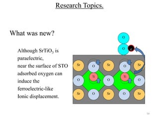
![This shows ALD process of Strontium Titanate thin film, (20-
nm-thick) which is used for novel oxygen sensor [T. Hara et
al., Sens. Actuators B 136 (2009) 489.].
32](https://image.slidesharecdn.com/msephdlecture-140921041805-phpapp01/85/Mse-phd-lecture-32-320.jpg)

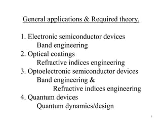
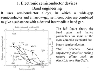
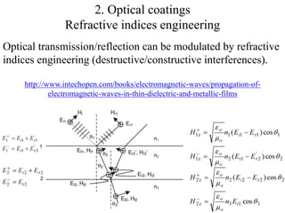
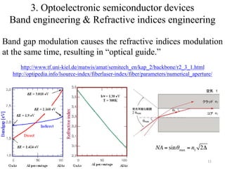
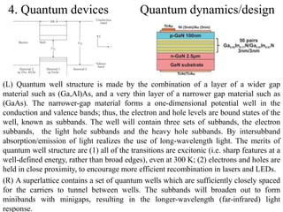
The document provides an overview of a lecture on thin film deposition techniques given by Dr. Toru Hara. It discusses four main applications of thin films: 1) electronic semiconductor devices using band engineering, 2) optical coatings using refractive index engineering, 3) optoelectronic devices using both band and refractive index engineering, and 4) quantum devices using quantum dynamics design. It also describes common thin film deposition methods including chemical solution deposition, chemical vapor deposition, plating, and physical vapor deposition techniques and gives examples of their use in applications such as transistors, optical coatings, LEDs, and superlattices.


![Thin_Film_Technology_introduction[1]](https://cdn.slidesharecdn.com/ss_thumbnails/1b4496c8-2102-411b-8465-a3dd3f398327-150205034538-conversion-gate02-thumbnail.jpg?width=640&height=640&fit=bounds)


