Downloaded 82 times

![HIGH K DIELECTRIC
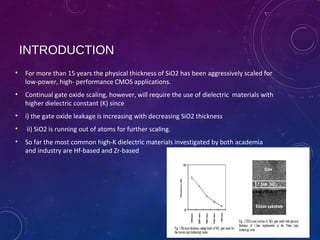
• Introducing higher dielectric constant (k > 10) insulators [mainly
transition metal (TM) oxides] is therefore indispensable for the 70
nm technology node and beyond
• TM silicates such as HfSiOx have been preferred because they have
better thermal stability compared to their oxides. The dielectric
constant of TM silicates is less than TM oxides but higher than silicon
oxide.](https://image.slidesharecdn.com/highk-dielectric-150406025506-conversion-gate01/85/High-k-dielectric-4-320.jpg)
![BIBLIOGRAPHY
•
References
• [1] S. Thompson et al., IEDM Technical Digest, p.61, 2002.
• [2] R. Chau et al., IEDM Technical Digest, p.45, 2000.
• [3] R. Chau et al., Physica E, Low-dimensional Systems and Nanostructures,
Vol. 19, Issues 1-2, p.1, July 2003.
• [4] S. Inumiya et al., Symp. of VLSI Technology, p.17, 2003.
• [5] G. Lucovsky et al., IEDM Technical Digest, p.617, 2002.
• [6] C. Hobbs et al., Symp. of VLSI Technology, p.9, 2003
• [7] M. Fischetti et al., J. Appl. Phys., Vol. 90, p.4587, 2001.
• [8] S. Datta et al., IEDM Technical Digest, p.653, 2003.
• [9] Q. Lu et al., Symp. of VLSI Technology, p.72, 2000.
• [10] R. Chau et al., Extended Abstracts of International Workshop on Gate
Insulator (IWGI), Tokyo, Japan, p.124, Nov. 2003.](https://image.slidesharecdn.com/highk-dielectric-150406025506-conversion-gate01/85/High-k-dielectric-16-320.jpg)

The document discusses the transition to high-k dielectrics in CMOS technology, addressing the need for materials with higher dielectric constants due to the limitations of traditional SiO2. It outlines the compatibility issues, performance challenges, and recent advancements in metal gate/high-k dielectric stacks that achieve excellent transistor performance with minimal leakage. Additionally, it highlights the application of high-k dielectrics in DRAM and ferroelectric memories, showcasing their benefits in high-speed, low-power electronic devices.


![Thin_Film_Technology_introduction[1]](https://cdn.slidesharecdn.com/ss_thumbnails/1b4496c8-2102-411b-8465-a3dd3f398327-150205034538-conversion-gate02-thumbnail.jpg?width=640&height=640&fit=bounds)