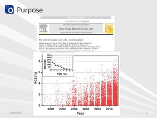
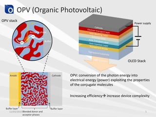
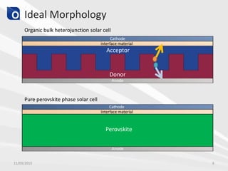
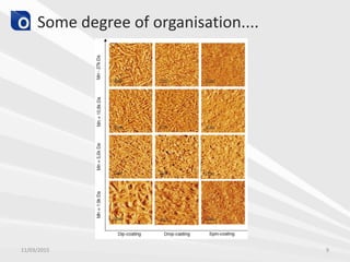
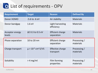
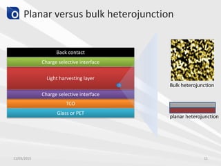
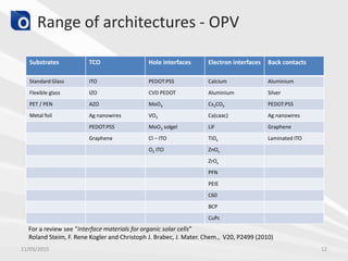
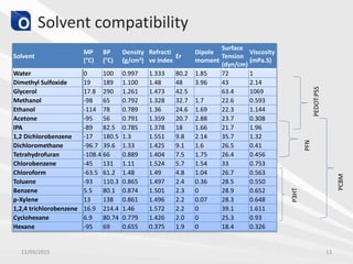
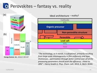
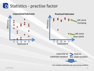
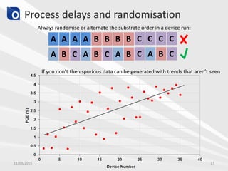
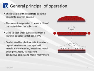
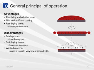
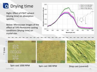
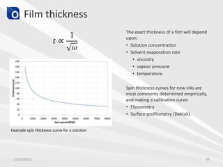
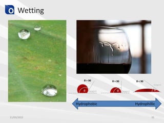
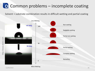
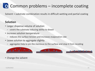
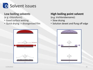
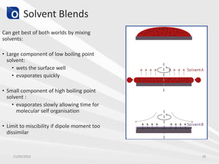
This document discusses considerations for organic photovoltaic (OPV) thin-film processing and spin coating. It addresses general OPV requirements, practical fabrication issues like cleaning and solvent compatibility, and spin coating parameters that influence film thickness and morphology such as solution concentration, spin speed, and solvent selection. The ideal is to use solvent blends that allow for good surface wetting and rapid drying while also permitting molecular self-organization in the film. Processing conditions like atmosphere, temperature, and substrate treatment are also crucial factors for technologies like perovskite solar cells.

![Morphology
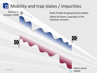
E
v
Ev
v: velocity of the carrier,
E=VDS/L: electrical field across the OSC
μ: Carrier mobility; [μ] =cm2/(V·s)
11/03/2015 8
- Long-Chain Polymeric OSC](https://image.slidesharecdn.com/maxreinhardt-liverpool04-11-14-150311054407-conversion-gate01/85/Organic-Photovoltaics-Thin-Film-Processing-Considerations-8-320.jpg)


![synthesis of semiconducting polymers for possible application in [autosaved]](https://cdn.slidesharecdn.com/ss_thumbnails/2-140822115954-phpapp02-thumbnail.jpg?width=640&height=640&fit=bounds)


![Polymer [ बहुलक ] Chemistry Notes PDF - Irfanullah Mehar - JJ Sir Chemistry.pdf](https://cdn.slidesharecdn.com/ss_thumbnails/polymerchemistrynotespdf-irfanullahmehar-jjsirchemistry-260210172118-3f9b37f7-thumbnail.jpg?width=640&height=640&fit=bounds)


