Download as PDF, PPTX


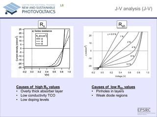
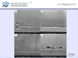
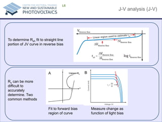
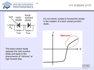
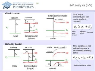
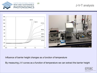
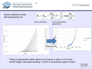
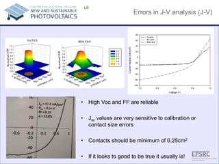
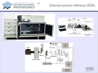
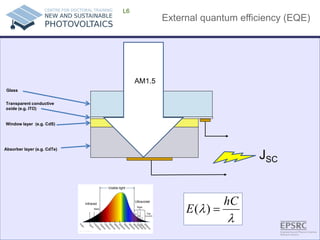
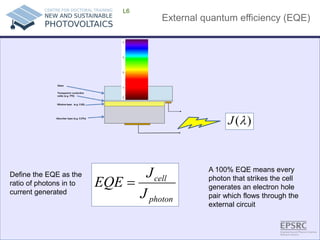
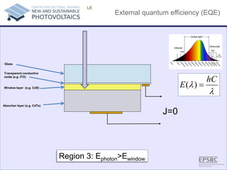
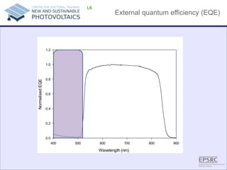
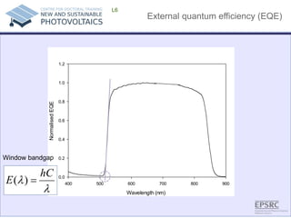
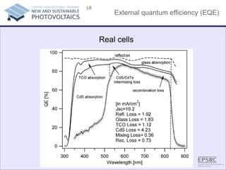
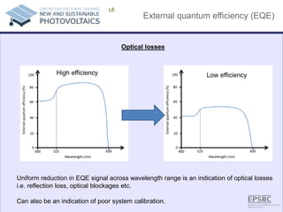
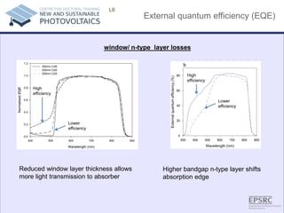
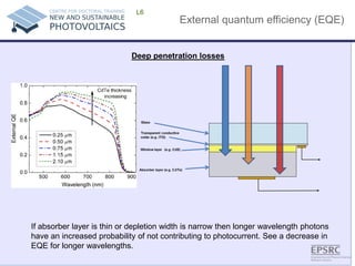
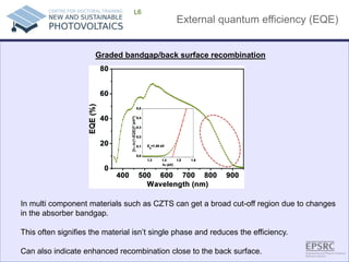
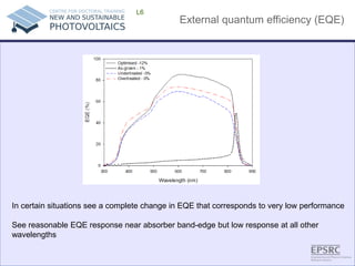
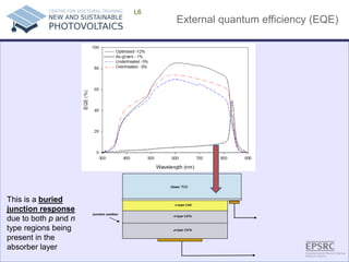
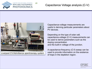
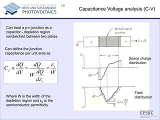
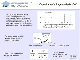
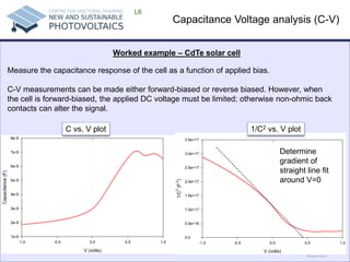
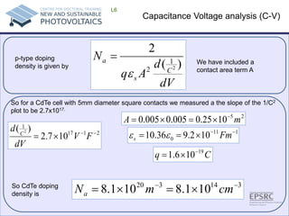
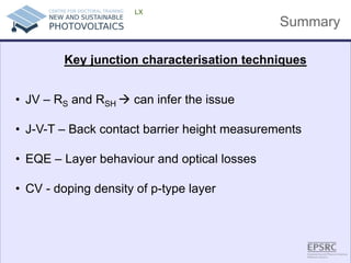

The document discusses junction characterization techniques in photovoltaic (PV) research, focusing on methods like current-voltage (J-V) analysis, external quantum efficiency (EQE) measurements, and capacitance-voltage (C-V) measurements. Key factors affecting solar cell performance such as series and shunt resistances, optical losses, and doping concentration are explored. The document emphasizes the importance of accurate measurements and the interpretation of results to enhance solar cell efficiency.


