Download as PDF, PPTX

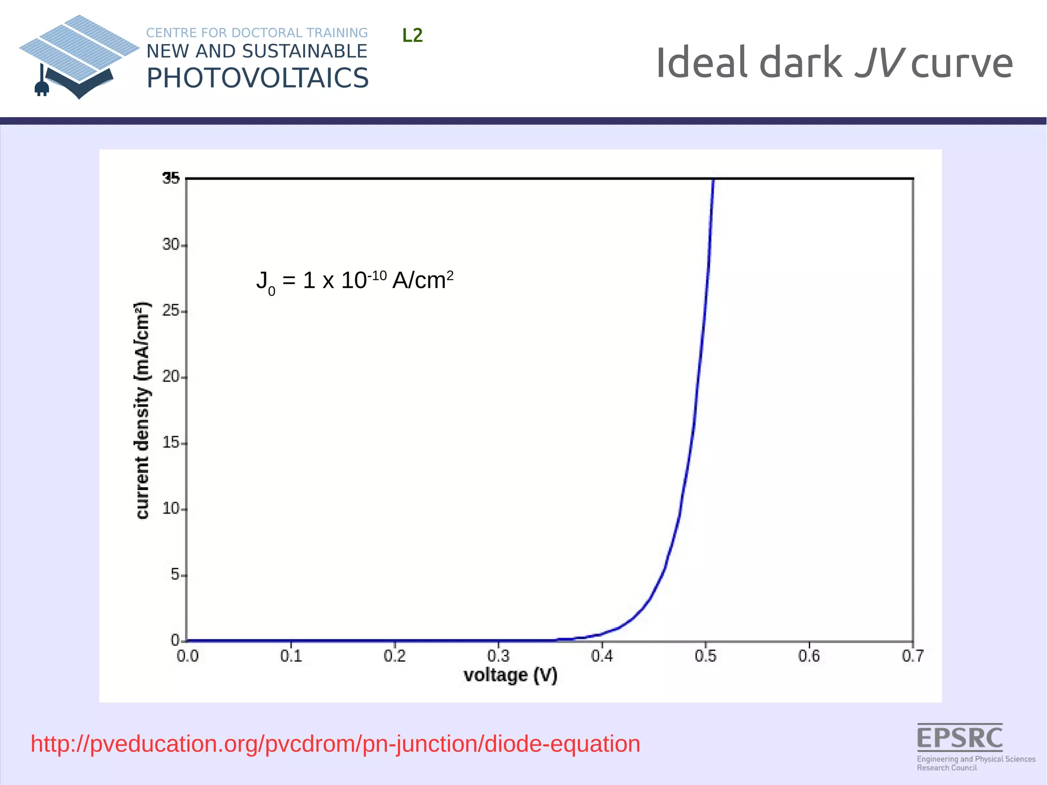
![Ideal Diode Equation
L2
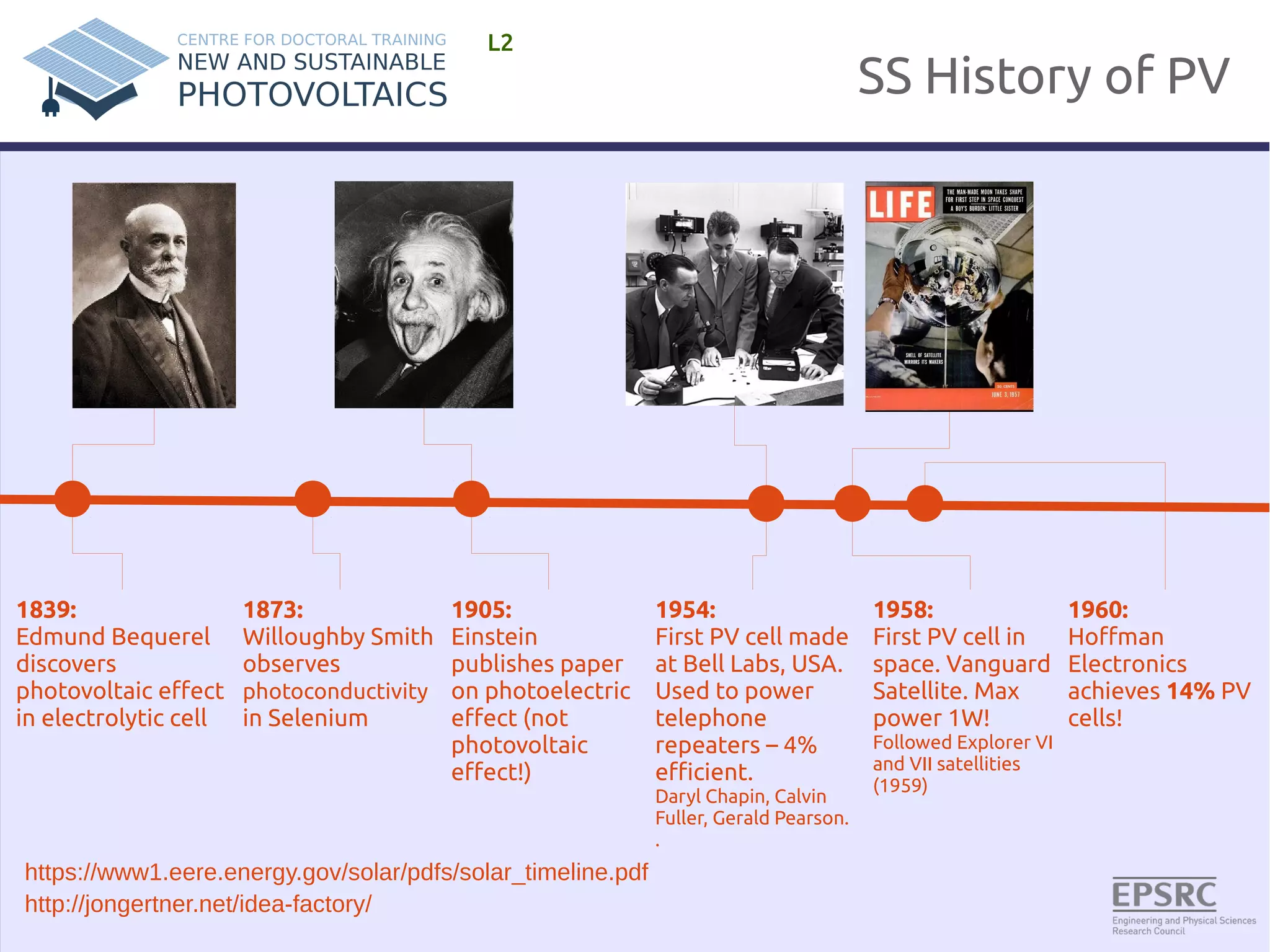
William Shockley:
Co-inventor of the transistor
with Bardeen and Brattain 1948
Nobel Prize: 1956
(Also a eugenicist)
Often called the Shockley equation:
J=J 0 [exp( eV
k BT )−1 ]
J0 – Dark saturation current.
V – applied voltage across the terminals of the diode
e – Electronic charge
kB – Boltzmann's constant
T – Absolute temperature (K)
Might derive this later for fun! (L5)
If every you need some inspiration: Read this!
http://books.google.co.uk/books/about/The_Idea_Factory.html?id=uOMt_XCo81QC&redir_esc=y](https://image.slidesharecdn.com/lecture22-141019075759-conversion-gate01/75/Fundamentals-of-Photovoltaics-Lecture-1-15-2048.jpg)
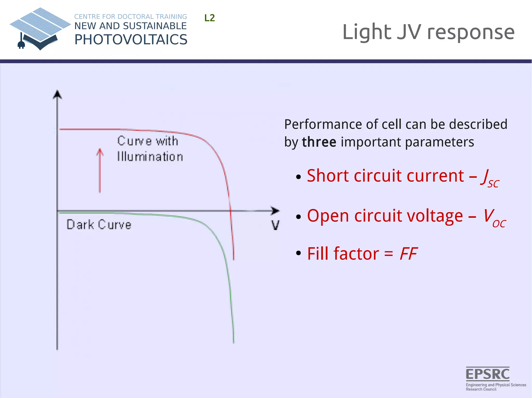
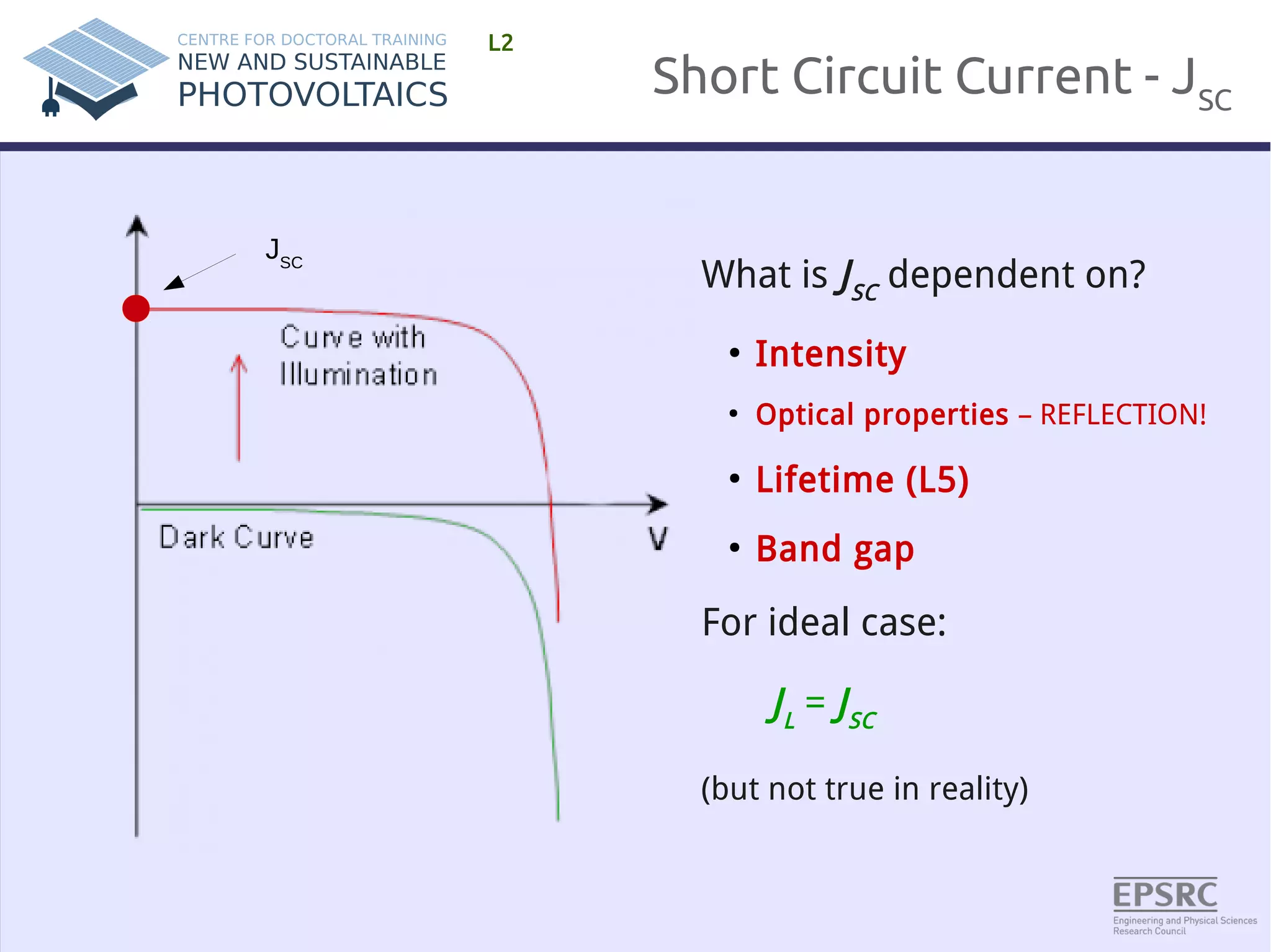
![Ideal diode for solar cell
L2
Sign convention: Lets say that the direction of a generated photo-current JL is
positive with respect to a negative dark current Jdark
J=J L−J dark
J=J L−J 0 [exp( eV
k BT )−1]
Equivalent Circuit:
Ideal solar cell](https://image.slidesharecdn.com/lecture22-141019075759-conversion-gate01/75/Fundamentals-of-Photovoltaics-Lecture-1-17-2048.jpg)
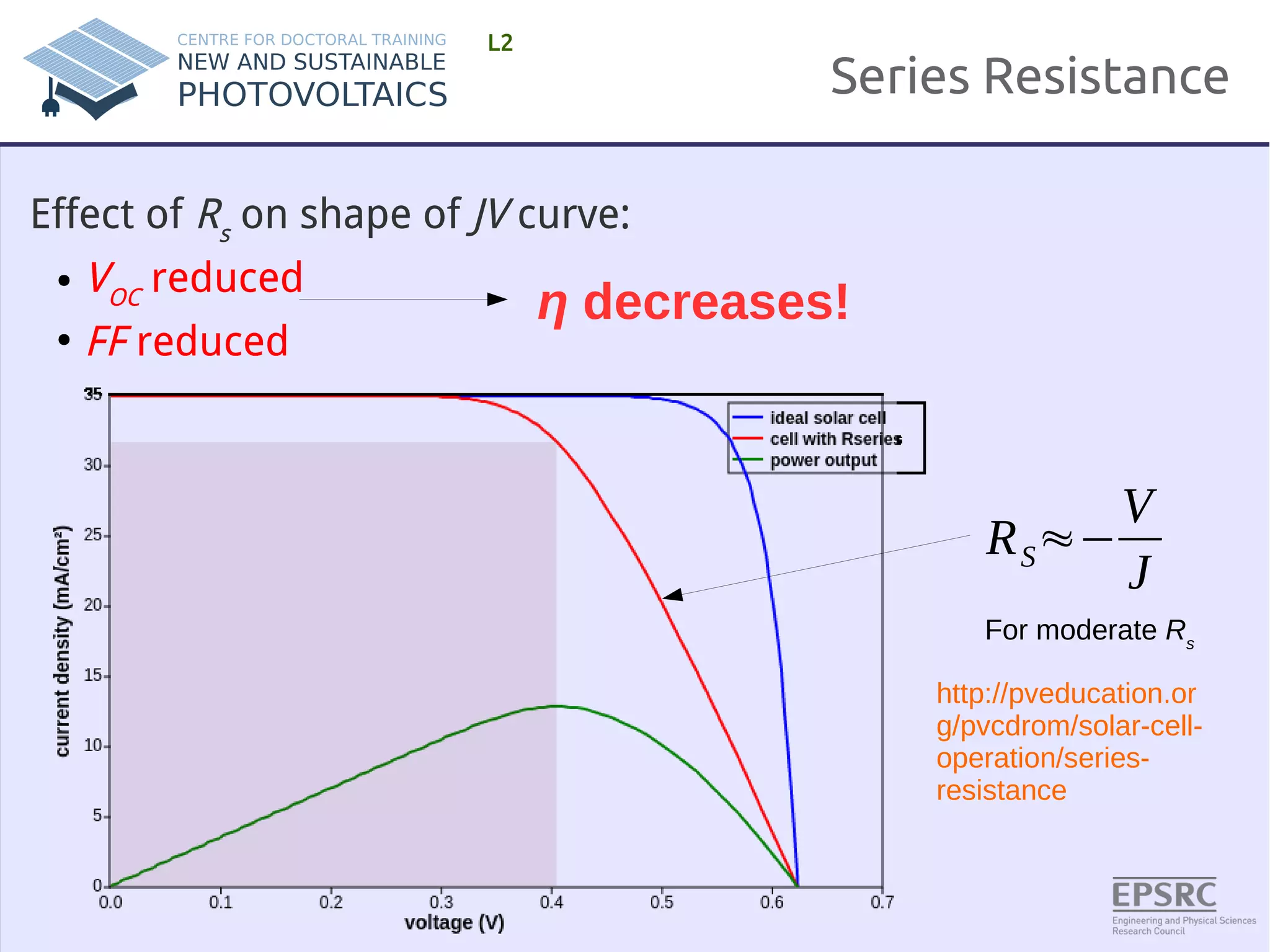
![Series Resistance, Rs
L2
Origin of series resistance in solar cell:
● Simply a property of real materials – i.e. non infinite mobility
● Resistances associated with back and front contacts to cell
Can represent sum of series resistance effects in equivalent circuit
using a single resistor in series:
Rs
J=J L−J 0 [exp(e (V +JRs)
kBT )−1] Uh oh!
Recursive Equation!](https://image.slidesharecdn.com/lecture22-141019075759-conversion-gate01/75/Fundamentals-of-Photovoltaics-Lecture-1-24-2048.jpg)
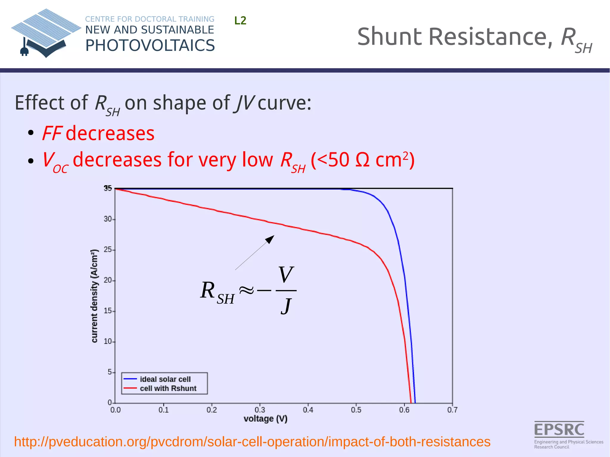
![Shunt Resistance, RSH
L2
Origin of shunt resistance in solar cell:
● Usually the result of poor fabrication methods
● Short circuit paths between electrodes of cell
Can represent sum of shunts in equivalent circuit using a single
resistor in parallel to diode:
J=J L−J 0 [exp(e (V +JRs)
kBT )−1]−
V +JRS
RSH](https://image.slidesharecdn.com/lecture22-141019075759-conversion-gate01/75/Fundamentals-of-Photovoltaics-Lecture-1-26-2048.jpg)
![Ideality Factor
L2
No such thing as an ideal diode
J=J 0 [exp( eV
nk BT )−1]
● n – typically takes values of between 1 and 2 (but can be higher)
● Originally used as a fudge factor for empirical data
● Now understood to be related to quality of SC material
● Related to carrier recombination (L4)](https://image.slidesharecdn.com/lecture22-141019075759-conversion-gate01/75/Fundamentals-of-Photovoltaics-Lecture-1-28-2048.jpg)

The document outlines a 3-day course on fundamentals of photovoltaics. Day 1 covers the history of solar cells, the photovoltaic effect, the AM1.5 solar spectrum, ideal diode equations, J-V curves, quantum efficiency and parasitic resistances. Day 2 focuses on semiconductors, junctions and their characterization. Day 3 discusses materials stability, optical properties, characterization techniques and current/future PV technologies, with an exam scheduled for Day 4.


