Downloaded 2,923 times
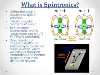
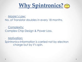
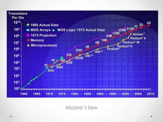
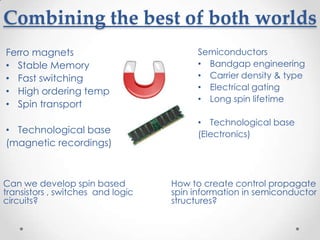
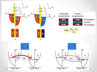
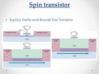
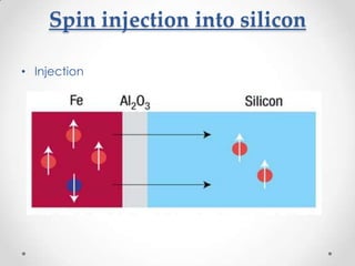
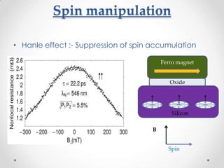
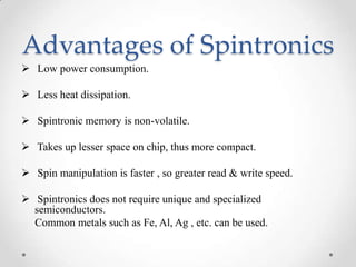


Spintronics utilizes the spin property of electrons to carry information. It offers advantages over traditional electronics like lower power consumption and greater density. Key developments include the giant magnetoresistance effect, spin transistors, and magnetic random access memory (MRAM). Continued research aims to better inject, manipulate, and detect electron spin in semiconductors for applications in memory and logic devices.