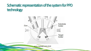
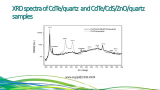
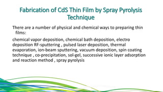
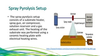
CdTe/CdS thin film
in Solar Cell
By: Zahra Behboodi “Master Student-Nano Physics”
Advisor :Dr. Zohreh Qurannevis
The presentation for the Course “Analysis of Nano Structure”
22th December 2015
–
Science & Research Branch
Outlines:
 Introduction to Cadmium telluride photovoltaics
 How a CdTe Solar Cell works?
 Fabrication of CdS Thin Film by Spray Pyrolysis Technique CdTe
layers deposited by Pulsed Plasma
Deposition (PPD)
 References
Cadmium telluride CdTe
• Structure:
• Crystal Structure
• Direct Band Gap Semiconductor:
1.5 eV
• Can be growth both p-type
and n-type
https://upload.wikimedia.org/wikipedia/commons/thumb/
2/22/Sphalerite-unit-cell-depth-fade-3D-balls.png/200px-
Sphalerite-unit-cell-depth-fade-3D-balls.png
Cadmium telluride photovoltaics
• Cadmium telluride (CdTe) photovoltaics describes a
photovoltaic (PV) technology that is based on the use
of cadmium telluride, a thin semiconductor layer
designed to absorb and convert sunlight into
electricity
• Cadmium telluride PV is the only thin film technology
with lower costs than conventional solar cells made of
crystalline silicon.
• upload.wikimedia.org/wikipedia/commons/thumb/5/5b/N
REL_Array.jpg/300px-NREL_Array.jpg
cadmium telluride (CdTe) solar panel
The Structure of a CdTe/CdS Sollar Cell
How a CdTe Solar Cell works?
http://finestsolar.co.uk/uploads/images/content-images/power-generation-01.jpg
Fabrication of CdS Thin Film by Spray Pyrolysis
Technique
There are a number of physical and chemical ways to preparing thin
films:
chemical vapor deposition, chemical bath deposition, electro
deposition RF-sputtering , pulsed laser deposition, thermal
evaporation, ion-beam sputtering, vacuum deposition, spin coating
technique , co-precipitation, sol-gel, successive ionic layer adsorption
and reaction method , spray pyrolysis
Comparison Spray Pyrolysis with other
Techniques
• Compared with other above mentioned techniques
spray pyrolysis is very simple, fast, low-cost method
and get uniform deposition of the films
Spray Pyrolysis Setup
• The spray pyrolysis setup
consists of a substrate heater,
spray gun, air compressor,
solution reservoir and a gas
exhaust unit. The heating of the
substrate was performed using a
ceramic heating plate with
electrical heating wires.
http://www.hindawi.com/journals/isrn/2012/275872.fig.002.jpg
Solution Preparation
• The precursor solution used for Cadmium sulphide thin films was
obtained by dissolving the salts of cadmium chloride and
Thioacetamide in the molar ratio of 1:2 in double distilled water,
ammonia as complexing agent and N, N-DMF as a solvent were
added drop by drop. The amount of solution was made to 50 ml.
Cadmium Chloride [CdCl2.2H2O] and Thioacetamide[CH3CSNH2 ]
Spray Process & Parameters for Spray Pyrolysis
• Spray Process
• The aqueous solution was then
sprayed on the preheated glass
substrate maintained at different
temperatures 250°C, 300°C and
350°C by conventional chemical
spray pyrolysis technique to
obtain homogeneous thin films
• Parameters for Spray
• (a) Type of salt: water soluble,
(b) Air pressure: 15 Kg/cm3, (c)
Deposition spray rate: 2.5
Kg/cm3, (d) Substrate
temperature: 250°C, 300°C &
350°C, (e) Nozzle to substrate
• distance: 20 Cm, (f) Spray time: 5
Sec, (g) Repeated cycles: 2
minutes,
Movie Showing Spray Pyrolysis
https://www.youtube.com/watch?v=eJbuY4HJFV0
Structural Properties / X-ray diffraction
patterns of the CdS thin films
• They are polycrystalline
hexagonal structures. Film
formations have a single peak
represented at 25° with planes
oriented in (1 0 0) direction and
it has good agreement with
standard X-ray diffraction data
which was reported in JCPDS
card number 02 – 0549.
Figure 1: XRD pattern of CdS thin films at different
substrate temperatures
Structural Properties / X-ray diffraction
patterns of the CdS thin films …
• The obtained average grain size was 11 nm, 18 nm and 22 nm for
250°C, 300°C and 350°C respectively. The peaks became sharper by
increasing the substrate temperature which indicates that as the
average grain size decreases.
Temperature increases the quality of the film
The AFM images of CdS thin films
The film obtained at substrate temperature of 250°C shows that it has dense structure with
un-even distribution of particles. At substrate temperature of 300°C the film exhibits rough
surface and strips like structures. The image at 350°C substrate temperature possess that
the film is homogeneous and plain, showing without any cracks.
• Reporting the results of the new deposition technique, Pulsed Plasma
Deposition (PPD), for the growth of the CdTe layers on
CdS/ZnO/quartz and quartz substrates. The PPD method allows to
deposit at low temperature. The optical band gap of deposited layers
is 1.50 eV, in perfect accord with the value
What is PPD?
• It is the technology based on the production of the pulsed plasma
accompanied by the generation of high energy electron pulses(up to
20 keV) directed to the source of deposited material (target). Electron
and plasma beam interaction with target generates the target
material plasma which propagates towards the substrate and deposits
on its surface.
• This technique, due to simple and compact electron gun construction
and high deposition rates, can be easily adapted to large area
deposition and represents a new choice for industrial production.
How Dees PPD Works?
The core of the PPD system is an electron gun generating the
pulsed beam of plasma and highenergy
electrons (up to 20 keV). The plasma and electron beam is created
from working gas (e.g.oxygen, argon or nitrogen) flowing at low
pressures (10-6 - 10-2 mbar) through the gun operational
body.
How Dees PPD Works? …
electron packet (impulse) on the target surface causes the energy
transfer from the beam into the target material and, consequently, the
target ablation. In other words, the explosion of the target surface in
the form of the target material plasma (plume) which propagates in the
direction of the substrate where it is deposited
SchematicrepresentationofthesystemforPPD
technology
arxiv.org/pdf/1103.4539
XRDspectraofCdTe/quartz andCdTe/CdS/ZnO/quartz
samples
arxiv.org/pdf/1103.4539
XRDspectraofCdTe/quartz andCdTe/CdS/ZnO/quartz samples…
• Figure shows that in both systems the CdTe film exhibits a
polycrystalline cubic phase (S.G.= F43m (216), a= 6.48 Ǻ, ICSD #:
043712), as determined by the analysis of the Bragg peak positions.
• The grain sizes of the CdTe, estimated by the FWHM of the peaks
applying the Debye-Sherrer Equation resulted to be of the same order
of magnitude, roughly 30 nm for both samples.
• The crystallinity of the CdTe film is largely affected by the nature of the
underneath layer. The degree of the crystallinity is lower for the CdTe
film deposited on the CdS substrate than that one for the CdTe film
grown on the quartz substrate, as suggested by the lack of numerous
reflections in the pattern of the CdTe/CdS spectra otherwise observed
for the CdTe/quartz.
References:
• www.ijsr.net/conf/ATOM2014/ATOM2014_07.pdf
• arxiv.org/pdf/1103.4539
• thesis.um.ac.ir/moreinfo-53720-pg-1.html
• https://en.wikipedia.org/wiki/Cadmium_telluride_photovoltaics

CdTe-CdS thin film in Solar Cell

  • 1.
    CdTe/CdS thin film inSolar Cell By: Zahra Behboodi “Master Student-Nano Physics” Advisor :Dr. Zohreh Qurannevis The presentation for the Course “Analysis of Nano Structure” 22th December 2015 – Science & Research Branch
  • 2.
    Outlines:  Introduction toCadmium telluride photovoltaics  How a CdTe Solar Cell works?  Fabrication of CdS Thin Film by Spray Pyrolysis Technique CdTe layers deposited by Pulsed Plasma Deposition (PPD)  References
  • 3.
    Cadmium telluride CdTe •Structure: • Crystal Structure • Direct Band Gap Semiconductor: 1.5 eV • Can be growth both p-type and n-type https://upload.wikimedia.org/wikipedia/commons/thumb/ 2/22/Sphalerite-unit-cell-depth-fade-3D-balls.png/200px- Sphalerite-unit-cell-depth-fade-3D-balls.png
  • 4.
    Cadmium telluride photovoltaics •Cadmium telluride (CdTe) photovoltaics describes a photovoltaic (PV) technology that is based on the use of cadmium telluride, a thin semiconductor layer designed to absorb and convert sunlight into electricity • Cadmium telluride PV is the only thin film technology with lower costs than conventional solar cells made of crystalline silicon. • upload.wikimedia.org/wikipedia/commons/thumb/5/5b/N REL_Array.jpg/300px-NREL_Array.jpg cadmium telluride (CdTe) solar panel
  • 5.
    The Structure ofa CdTe/CdS Sollar Cell
  • 6.
    How a CdTeSolar Cell works? http://finestsolar.co.uk/uploads/images/content-images/power-generation-01.jpg
  • 7.
    Fabrication of CdSThin Film by Spray Pyrolysis Technique There are a number of physical and chemical ways to preparing thin films: chemical vapor deposition, chemical bath deposition, electro deposition RF-sputtering , pulsed laser deposition, thermal evaporation, ion-beam sputtering, vacuum deposition, spin coating technique , co-precipitation, sol-gel, successive ionic layer adsorption and reaction method , spray pyrolysis
  • 8.
    Comparison Spray Pyrolysiswith other Techniques • Compared with other above mentioned techniques spray pyrolysis is very simple, fast, low-cost method and get uniform deposition of the films
  • 9.
    Spray Pyrolysis Setup •The spray pyrolysis setup consists of a substrate heater, spray gun, air compressor, solution reservoir and a gas exhaust unit. The heating of the substrate was performed using a ceramic heating plate with electrical heating wires. http://www.hindawi.com/journals/isrn/2012/275872.fig.002.jpg
  • 10.
    Solution Preparation • Theprecursor solution used for Cadmium sulphide thin films was obtained by dissolving the salts of cadmium chloride and Thioacetamide in the molar ratio of 1:2 in double distilled water, ammonia as complexing agent and N, N-DMF as a solvent were added drop by drop. The amount of solution was made to 50 ml. Cadmium Chloride [CdCl2.2H2O] and Thioacetamide[CH3CSNH2 ]
  • 11.
    Spray Process &Parameters for Spray Pyrolysis • Spray Process • The aqueous solution was then sprayed on the preheated glass substrate maintained at different temperatures 250°C, 300°C and 350°C by conventional chemical spray pyrolysis technique to obtain homogeneous thin films • Parameters for Spray • (a) Type of salt: water soluble, (b) Air pressure: 15 Kg/cm3, (c) Deposition spray rate: 2.5 Kg/cm3, (d) Substrate temperature: 250°C, 300°C & 350°C, (e) Nozzle to substrate • distance: 20 Cm, (f) Spray time: 5 Sec, (g) Repeated cycles: 2 minutes,
  • 12.
    Movie Showing SprayPyrolysis https://www.youtube.com/watch?v=eJbuY4HJFV0
  • 13.
    Structural Properties /X-ray diffraction patterns of the CdS thin films • They are polycrystalline hexagonal structures. Film formations have a single peak represented at 25° with planes oriented in (1 0 0) direction and it has good agreement with standard X-ray diffraction data which was reported in JCPDS card number 02 – 0549. Figure 1: XRD pattern of CdS thin films at different substrate temperatures
  • 14.
    Structural Properties /X-ray diffraction patterns of the CdS thin films … • The obtained average grain size was 11 nm, 18 nm and 22 nm for 250°C, 300°C and 350°C respectively. The peaks became sharper by increasing the substrate temperature which indicates that as the average grain size decreases. Temperature increases the quality of the film
  • 15.
    The AFM imagesof CdS thin films The film obtained at substrate temperature of 250°C shows that it has dense structure with un-even distribution of particles. At substrate temperature of 300°C the film exhibits rough surface and strips like structures. The image at 350°C substrate temperature possess that the film is homogeneous and plain, showing without any cracks.
  • 16.
    • Reporting theresults of the new deposition technique, Pulsed Plasma Deposition (PPD), for the growth of the CdTe layers on CdS/ZnO/quartz and quartz substrates. The PPD method allows to deposit at low temperature. The optical band gap of deposited layers is 1.50 eV, in perfect accord with the value
  • 17.
    What is PPD? •It is the technology based on the production of the pulsed plasma accompanied by the generation of high energy electron pulses(up to 20 keV) directed to the source of deposited material (target). Electron and plasma beam interaction with target generates the target material plasma which propagates towards the substrate and deposits on its surface. • This technique, due to simple and compact electron gun construction and high deposition rates, can be easily adapted to large area deposition and represents a new choice for industrial production.
  • 18.
    How Dees PPDWorks? The core of the PPD system is an electron gun generating the pulsed beam of plasma and highenergy electrons (up to 20 keV). The plasma and electron beam is created from working gas (e.g.oxygen, argon or nitrogen) flowing at low pressures (10-6 - 10-2 mbar) through the gun operational body.
  • 19.
    How Dees PPDWorks? … electron packet (impulse) on the target surface causes the energy transfer from the beam into the target material and, consequently, the target ablation. In other words, the explosion of the target surface in the form of the target material plasma (plume) which propagates in the direction of the substrate where it is deposited
  • 20.
  • 21.
  • 22.
    XRDspectraofCdTe/quartz andCdTe/CdS/ZnO/quartz samples… •Figure shows that in both systems the CdTe film exhibits a polycrystalline cubic phase (S.G.= F43m (216), a= 6.48 Ǻ, ICSD #: 043712), as determined by the analysis of the Bragg peak positions. • The grain sizes of the CdTe, estimated by the FWHM of the peaks applying the Debye-Sherrer Equation resulted to be of the same order of magnitude, roughly 30 nm for both samples. • The crystallinity of the CdTe film is largely affected by the nature of the underneath layer. The degree of the crystallinity is lower for the CdTe film deposited on the CdS substrate than that one for the CdTe film grown on the quartz substrate, as suggested by the lack of numerous reflections in the pattern of the CdTe/CdS spectra otherwise observed for the CdTe/quartz.
  • 23.
    References: • www.ijsr.net/conf/ATOM2014/ATOM2014_07.pdf • arxiv.org/pdf/1103.4539 •thesis.um.ac.ir/moreinfo-53720-pg-1.html • https://en.wikipedia.org/wiki/Cadmium_telluride_photovoltaics