Proceedings of the 2nd International Conference on Current Trends in Engineering and Management ICCTEM -2014 
INTERNATIONAL JOURNAL OF ELECTRONICS AND 
17 – 19, July 2014, Mysore, Karnataka, India 
COMMUNICATION ENGINEERING  TECHNOLOGY (IJECET) 
ISSN 0976 – 6464(Print) 
ISSN 0976 – 6472(Online) 
Volume 5, Issue 8, August (2014), pp. 107-116 
© IAEME: http://www.iaeme.com/IJECET.asp 
Journal Impact Factor (2014): 7.2836 (Calculated by GISI) 
www.jifactor.com 
IJECET 
© I A E M E 
AN IMPROVISED DESIGN IMPLEMENTATION OF SRAM 
Poornima.H.S1, Deepu M2, Jyothi V3, Ajay.M.N4 
1Assistant Professor, Dept of ECE VVCE, Mysore 
2, 3, 4Student, Dept of VVCE, Mysore 
107 
ABSTRACT 
Memory arrays are an essential building block in any digital system. Static random-access 
memory (SRAM or static RAM) is a type of semiconductor memory that uses bistable latching 
circuitry to store each bit. The term static differentiates it from dynamic RAM (DRAM) which must 
be periodically refreshed. SRAM exhibits data remanence, but it is still volatile in the conventional 
sense that data is eventually lost when the memory is not powered. The aspects of designing an 
SRAM are very vital to designing other digital circuits as well. The majority of space taken in an 
integrated circuit is the memory. SRAM design consists of key considerations, such as increased 
speed and reduced layout area. This paper is aimed at creating an efficient SRAM design using 
Cadence. The focus was on developing simplified design by reducing the transistor count and 
replacing some of the conventional circuit designs. 
Keywords: Bistable Data Remanence, Volatile, Cadence. 
I. INTRODUCTION 
Static random-access memory (SRAM) is a type of semiconductor memory that uses 
bistable latching circuitry to store each bit. The term static differentiates it from dynamic RAM 
(DRAM) which must be periodically refreshed. SRAM exhibits data remanence. SRAM is designed 
to provide an interface with CPU and to replace DRAMs in systems that require very low power 
consumption. A SRAM cell must meet the requirements for the operation in submicron/nano ranges. 
The scaling of CMOS technology has significant impacts on SRAM cell – random fluctuation of 
electrical characteristics and substantial leakage current. 
II. SRAM ARRAY 
The basic architecture of a SRAM consists of an array of memory cells with support circuitry 
to decode addresses and implement the read and write operations. SRAM arrays are arranged in rows 
and columns of memory cells called wordlines and bitlines, respectively. Typically, the wordlines are
Proceedings of the 2nd International Conference on Current Trends in Engineering and Management ICCTEM -2014 
17 – 19, July 2014, Mysore, Karnataka, India 
made from poly silicon while the bitlines are metal. Each memory cell has a unique location or 
address defined by the intersection of a row and a column. 
108 
2.1 6T SRAM cell 
A typical SRAM cell comprises of two cross-coupled inverters forming a latch and two 
accesses. Essentially, the data is latched at the cross-coupled inverters. The bit-lines are 
complementary and are input to the I/O of the inverters. Thus, the value is latched during a write and 
maintained as long as power is available. 
2.2 Transistor sizing 
An SRAM Cell has to provide non-destructive read and a quick write-the two opposing 
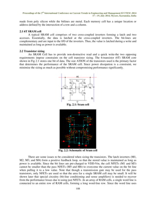
requirements impose constraints on the cell transistor sizing. The 6-transistor (6T) SRAM core 
shown in Fig 2.1 stores one bit of data. The size ATION of the transistors used is the primary factor 
that determines the performance of the SRAM cell. Since power dissipation is a constraint, we 
minimize the sizing as much as possible without compromising performance significantly. 
Fig. 2.1: Sram cell 
Fig. 2.2: Schematic of Sram cell 
There are some issues to be considered when sizing the transistors. The latch inverters (M1, 
M2, M3, and M4) form a positive feedback loop, so that the stored value is maintained as long as 
power is available. Since the bit lines are pre-charged to VDD-Vtn, the cell NFETs (M1 and M3) 
cannot be smaller than the pass NFETs (M5 and M6) to overcome the current value on the bit line 
when pulling it to a low value. Note that though a transmission gate may be used for the pass 
transistors, only NFETs are used so that the area for a single SRAM cell may be small. It will be 
shown later that special circuitry (bit-line conditioning and sense amplifiers) is needed to recover 
from the performance losses due to using just NFETs .In an array of RAM cells, a single word line is 
connected to an entire row of RAM cells, forming a long word-line row. Since the word line uses
Proceedings of the 2nd International Conference on Current Trends in Engineering and Management ICCTEM -2014 
17 – 19, July 2014, Mysore, Karnataka, India 
poly silicon (which has high resistivity), it is necessary to keep the two pass transistors (M5 and M6) 
small. This improves signal integrity on the word lines and reduces power dissipation. Therefore, the 
size is kept small. 
During the read operation, it was concluded that transistor Q1 had to be stronger than 
transistor Q5 to prevent accidental writing. Now in the write case, this feature actually prevents a 
wanted write operation. Even when transistor Q5 is turned on and current is flowing from BL to the 
storage node, the state of the node will not change. As soon as the node is raised transistor Q1 will 
sink current to ground, and the node is prevented from reaching even close to the switching point. So 
instead of writing a ’1’ to the node, a ’0’ will be written to the inverse node. Looking at the right side 
of the cell we have the constellation Q4-Q6. In this case BLB is held at gnd. When the wordline is 
raised Q6 is turned on and current is drawn from the inverse storage node to BLB. 
At the same time, however, Q4 is turned on and, as soon as the potential at the inverse 
storage node starts to decrease, current will flow from VDD to the node. In this case Q6 has to be 
stronger than Q4 for the inverse node to change its state. The transistor Q4 is a PMOS Transistor and 
inherently weaker than the NMOS transistor Q6 (the mobility is lower in PMOS than in NMOS). 
The Sram array is functionally divided into four blocks 
109 
• I/O section 
• Decoder Section 
• Control section 
III. I/o SECTION 
This section of SRAM is responsible for pre-charging bitlines, sensing differential analog 
voltage during read operation and driving bitlines during write operation. It has the following 
functional blocks. 
• Pre-charge 
• Sense Amplifier 
• Write Amplifier 
3.1 Pre-charge circuit 
The pre-charge circuit ensures charging of bitlines before read operation. When two RAM 
cells containing opposite value in the same columns are accessed subsequently, the output has to 
switch first to an equalized state and then to the opposite logic state. Since the capacitance on the bit 
lines is quite large, the time required for switching the differential from one state to the other 
becomes a significant portion of the overall access time. Equalization of the bit-lines between the 
accesses can reduce the access time. 
The size of the charge transistors must be as small as possible, so that they do not override 
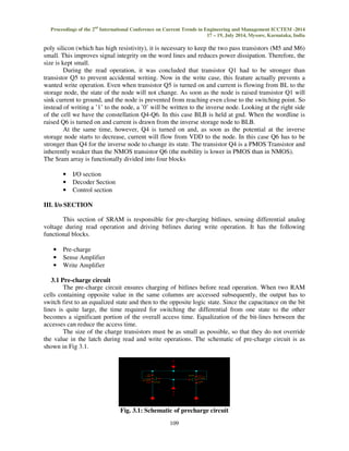
the value in the latch during read and write operations. The schematic of pre-charge circuit is as 
shown in Fig 3.1. 
Fig. 3.1: Schematic of precharge circuit
Proceedings of the 2nd International Conference on Current Trends in Engineering and Management ICCTEM -2014 
17 – 19, July 2014, Mysore, Karnataka, India 
110 
3.2 Sense Amplifier 
Sense amplifiers are an important component in memory design. The primary function of a 
sense amplifier in SRAMs is to amplify a small analog differential voltage developed on the bit lines 
by a read-accessed cell to the full swing digital output signal thus greatly reducing the time required 
for a read operation. Since SRAMs do not feature data refresh after sensing, the sensing operation 
must be non-destructive, as opposed to the destructive sensing of a DRAM cell. A sense amplifier 
allows the storage cells to be small, since each individual cell need not fully discharge the bit 
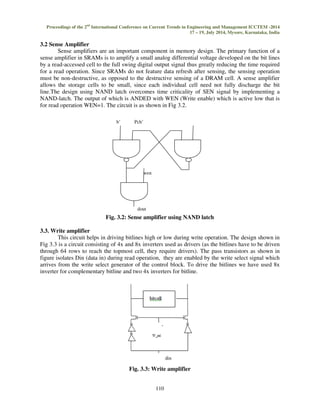
line.The design using NAND latch overcomes time criticality of SEN signal by implementing a 
NAND-latch. The output of which is ANDED with WEN (Write enable) which is active low that is 
for read operation WEN=1. The circuit is as shown in Fig 3.2. 
Pch’ 
Fig. 3.2: Sense amplifier using NAND latch 
3.3. Write amplifier 
This circuit helps in driving bitlines high or low during write operation. The design shown in 
Fig 3.3 is a circuit consisting of 4x and 8x inverters used as drivers (as the bitlines have to be driven 
through 64 rows to reach the topmost cell, they require drivers). The pass transistors as shown in 
figure isolates Din (data in) during read operation, they are enabled by the write select signal which 
arrives from the write select generator of the control block. To drive the bitlines we have used 8x 
inverter for complementary bitline and two 4x inverters for bitline. 
Fig. 3.3: Write amplifier 
b’ 
wen 
dout 
 
din
Proceedings of the 2nd International Conference on Current Trends in Engineering and Management ICCTEM -2014 
17 – 19, July 2014, Mysore, Karnataka, India 
111 
3.4 Decoder section 
The decoder decodes the input address to access the particular row. The multiple-stage 
decoding uses several hierarchically-linked blocks. Normally, the most significant bits are decoded 
(pre−decoded) in the first decoder stage, effectively selecting the array that is to be accessed by 
providing enable signals for the subsequent decoder stage(s) that enable a particular word line. The 
number of outputs of the last decoding stage corresponds to the number of rows (word lines) to be 
decoded 
A pre-decoder is used in the design to reduce the fan-in and the size of the NAND gate 
needed to create the decoder. This results in a faster decoder. For a 64x8 memory array that is 
designed, two stage decoding is chosen. 
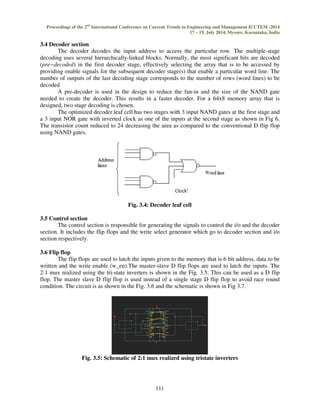
The optimized decoder leaf cell has two stages with 3 input NAND gates at the first stage and 
a 3 input NOR gate with inverted clock as one of the inputs at the second stage as shown in Fig 6. 
The transistor count reduced to 24 decreasing the area as compared to the conventional D flip flop 
using NAND gates. 
Fig. 3.4: Decoder leaf cell 
3.5 Control section 
The control section is responsible for generating the signals to control the i/o and the decoder 
section. It includes the flip flops and the write select generator which go to decoder section and i/o 
section respectively. 
3.6 Flip flop 
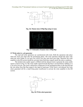
The flip flops are used to latch the inputs given to the memory that is 6 bit address, data to be 
written and the write enable (w_en).The master-slave D flip flops are used to latch the inputs. The 
2:1 mux realized using the tri-state inverters is shown in the Fig. 3.5. This can be used as a D flip 
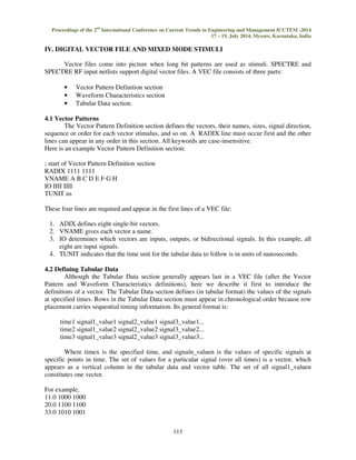
flop. The master slave D flip flop is used instead of a single stage D flip flop to avoid race round 
condition. The circuit is as shown in the Fig. 3.6 and the schematic is shown in Fig 3.7. 
Fig. 3.5: Schematic of 2:1 mux realized using tristate inverters
Proceedings of the 2nd International Conference on Current Trends in Engineering and Management ICCTEM -2014 
17 – 19, July 2014, Mysore, Karnataka, India 
Fig. 3.6: Master-slave D flip flop using 2:1 mux 
Fig. 3.7: Schematic of master-slave D flip flop 
112 
3.7 Write select (w_sel) generator 
The read and write operations are synchronized with clock. Both the operations take place 
when the clock goes high after the precharging phase. The write operation should take place only 
when the write enable (w_en) goes low (active low pin) and clock goes high. Therefore the write 
amplifier in the I/O section should be activated when both these signals satisfy the above conditions. 
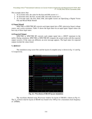
The latched write enable signal is ANDed with the delayed clock to generate the write enable 
signal as shown in Fig 3.8. The write enable signal from the flip flop is inverted before ANDing as it 
is an active low pin. The clock is delayed to compensate for the propagation delay in the flip flop and 
the wire delay from flip flop output to the input of nand gate. If the clock is not delayed, the write 
select generated will be a small firing pulse insufficient to activate the write amplifier in the I/O 
section. 
Fig. 3.8: Write select generator
Proceedings of the 2nd International Conference on Current Trends in Engineering and Management ICCTEM -2014 
17 – 19, July 2014, Mysore, Karnataka, India 
IV. DIGITAL VECTOR FILE AND MIXED MODE STIMULI 
Vector files come into picture when long bit patterns are used as stimuli. SPECTRE and 
SPECTRE RF input netlists support digital vector files. A VEC file consists of three parts: 
113 
• Vector Pattern Definition section 
• Waveform Characteristics section 
• Tabular Data section. 
4.1 Vector Patterns 
The Vector Pattern Definition section defines the vectors, their names, sizes, signal direction, 
sequence or order for each vector stimulus, and so on. A RADIX line must occur first and the other 
lines can appear in any order in this section. All keywords are case-insensitive. 
Here is an example Vector Pattern Definition section: 
; start of Vector Pattern Definition section 
RADIX 1111 1111 
VNAME A B C D E F G H 
IO IIII IIII 
TUNIT ns 
These four lines are required and appear in the first lines of a VEC file: 
1. ADIX defines eight single-bit vectors. 
2. VNAME gives each vector a name. 
3. IO determines which vectors are inputs, outputs, or bidirectional signals. In this example, all 
eight are input signals. 
4. TUNIT indicates that the time unit for the tabular data to follow is in units of nanoseconds. 
4.2 Defining Tabular Data 
Although the Tabular Data section generally appears last in a VEC file (after the Vector 
Pattern and Waveform Characteristics definitions), here we describe it first to introduce the 
definitions of a vector. The Tabular Data section defines (in tabular format) the values of the signals 
at specified times. Rows in the Tabular Data section must appear in chronological order because row 
placement carries sequential timing information. Its general format is: 
time1 signal1_value1 signal2_value1 signal3_value1... 
time2 signal1_value2 signal2_value2 signal3_value2... 
time3 signal1_value3 signal2_value3 signal3_value3... 
Where timex is the specified time, and signaln_valuen is the values of specific signals at 
specific points in time. The set of values for a particular signal (over all times) is a vector, which 
appears as a vertical column in the tabular data and vector table. The set of all signal1_valuen 
constitutes one vector. 
For example, 
11.0 1000 1000 
20.0 1100 1100 
33.0 1010 1001
Proceedings of the 2nd International Conference on Current Trends in Engineering and Management ICCTEM -2014 
17 – 19, July 2014, Mysore, Karnataka, India 
114 
This example shows that: 
1. At 11.0 time units, the value for the first and fifth vectors is 1. 
2. At 20.0 time units, the first, second, fifth, and sixth vectors are 1. 
3. At 33.0 time units, the first, third, fifth, and eighth vectors are Specifying a Digital Vector 
File and Mixed Mode Stimuli 
4.3 Input Stimuli 
SPECTRE or SPECTRE RF converts each input signal into a PWL (piecewise linear) voltage 
source, and a series resistance. Table 15 shows the legal states for an input signal. Signal values can 
have any of these legal states. 
4.4 Expected Output 
SPECTRE or SPECTRE RF converts each output signal into a .DOUT statement in the 
netlist. During simulation, SPECTRE or SPECTRE RF compares the actual results with the expected 
output vector(s). If the states are different, an error message appears. The legal states for expected 
outputs include the values listed. 
V. RESULT 
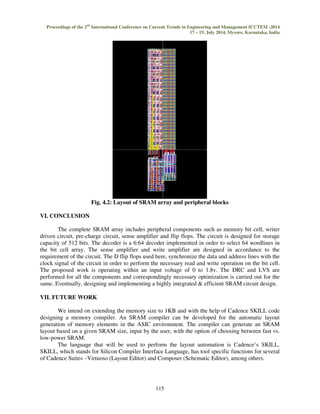
The simulation using vector files and the layout of complete array is shown in fig. 4.1 and fig. 
4.2 respectively. 
Fig. 4.1: Waveform of SRAM layout simulation 
The waveform obtained using Wavescan window for layout of SRAM is shown in Fig 4.1. 
The Tcq (Clock to Q) for layout of SRAM was found to be 1500 ps for a maximum clock frequency 
of 250MHz.
Proceedings of the 2nd International Conference on Current Trends in Engineering and Management ICCTEM -2014 
17 – 19, July 2014, Mysore, Karnataka, India 
Fig. 4.2: Layout of SRAM array and peripheral blocks 
115 
VI. CONCLUSION 
The complete SRAM array includes peripheral components such as memory bit cell, writer 
driven circuit, pre-charge circuit, sense amplifier and flip flops. The circuit is designed for storage 
capacity of 512 bits. The decoder is a 6:64 decoder implemented in order to select 64 wordlines in 
the bit cell array. The sense amplifier and write amplifier are designed in accordance to the 
requirement of the circuit. The D flip flops used here, synchronize the data and address lines with the 
clock signal of the circuit in order to perform the necessary read and write operation on the bit cell. 
The proposed work is operating within an input voltage of 0 to 1.8v. The DRC and LVS are 
performed for all the components and correspondingly necessary optimization is carried out for the 
same. Eventually, designing and implementing a highly integrated  efficient SRAM circuit design. 
VII. FUTURE WORK 
We intend on extending the memory size to 1KB and with the help of Cadence SKILL code 
designing a memory compiler. An SRAM compiler can be developed for the automatic layout 
generation of memory elements in the ASIC environment. The compiler can generate an SRAM 
layout based on a given SRAM size, input by the user, with the option of choosing between fast vs. 
low-power SRAM. 
The language that will be used to perform the layout automation is Cadence’s SKILL. 
SKILL, which stands for Silicon Compiler Interface Language, has tool specific functions for several 
of Cadence Suites –Virtuoso (Layout Editor) and Composer (Schematic Editor), among others.
Proceedings of the 2nd International Conference on Current Trends in Engineering and Management ICCTEM -2014 
17 – 19, July 2014, Mysore, Karnataka, India 
116 
VIII. ACKNOWLEDGEMENT 
First and foremost we pay our due regards to our renowned institution Vidyavardhaka 
College of Engineering, which provided us a platform and an opportunity for carrying out this work 
and our guide Sunil Kumar H V, layout team lead manager, Sankalp Semiconductors, Bangalore. 
IX. REFERENCES 
[1] Bhavya Daya, Shu Jiang, Piotr Nowak, Jaffer Sharief Synchronous 16x8 SRAM Design, 
Electrical Engineering Department, University of Florida. 
[2] Mehdi Alipour, Mostafa E. Salehi1, Hesamodin shojaei baghini, Design Space Exploration to 
Find the Optimum Cache and Register File Size for Embedded Applications Islamic Azad 
University. 
[3] Meenatchi Jagasivamani Development of a Low-Power SRAM Compiler Virginia Polytechnic 
Institute and State University. 
[4] Andrei Pavlov and Manoj Sachdev CMOS SRAM Circuit Design and Parametric Test in 
Nano-Scaled Technologies, Process-Aware SRAM Design and Test. 
[5] Andrei S Pavlov Design and test of embedded SRAMSs University of Waterloo.

An improvised design implementation of sram

  • 1.
    Proceedings of the2nd International Conference on Current Trends in Engineering and Management ICCTEM -2014 INTERNATIONAL JOURNAL OF ELECTRONICS AND 17 – 19, July 2014, Mysore, Karnataka, India COMMUNICATION ENGINEERING TECHNOLOGY (IJECET) ISSN 0976 – 6464(Print) ISSN 0976 – 6472(Online) Volume 5, Issue 8, August (2014), pp. 107-116 © IAEME: http://www.iaeme.com/IJECET.asp Journal Impact Factor (2014): 7.2836 (Calculated by GISI) www.jifactor.com IJECET © I A E M E AN IMPROVISED DESIGN IMPLEMENTATION OF SRAM Poornima.H.S1, Deepu M2, Jyothi V3, Ajay.M.N4 1Assistant Professor, Dept of ECE VVCE, Mysore 2, 3, 4Student, Dept of VVCE, Mysore 107 ABSTRACT Memory arrays are an essential building block in any digital system. Static random-access memory (SRAM or static RAM) is a type of semiconductor memory that uses bistable latching circuitry to store each bit. The term static differentiates it from dynamic RAM (DRAM) which must be periodically refreshed. SRAM exhibits data remanence, but it is still volatile in the conventional sense that data is eventually lost when the memory is not powered. The aspects of designing an SRAM are very vital to designing other digital circuits as well. The majority of space taken in an integrated circuit is the memory. SRAM design consists of key considerations, such as increased speed and reduced layout area. This paper is aimed at creating an efficient SRAM design using Cadence. The focus was on developing simplified design by reducing the transistor count and replacing some of the conventional circuit designs. Keywords: Bistable Data Remanence, Volatile, Cadence. I. INTRODUCTION Static random-access memory (SRAM) is a type of semiconductor memory that uses bistable latching circuitry to store each bit. The term static differentiates it from dynamic RAM (DRAM) which must be periodically refreshed. SRAM exhibits data remanence. SRAM is designed to provide an interface with CPU and to replace DRAMs in systems that require very low power consumption. A SRAM cell must meet the requirements for the operation in submicron/nano ranges. The scaling of CMOS technology has significant impacts on SRAM cell – random fluctuation of electrical characteristics and substantial leakage current. II. SRAM ARRAY The basic architecture of a SRAM consists of an array of memory cells with support circuitry to decode addresses and implement the read and write operations. SRAM arrays are arranged in rows and columns of memory cells called wordlines and bitlines, respectively. Typically, the wordlines are
  • 2.
    Proceedings of the2nd International Conference on Current Trends in Engineering and Management ICCTEM -2014 17 – 19, July 2014, Mysore, Karnataka, India made from poly silicon while the bitlines are metal. Each memory cell has a unique location or address defined by the intersection of a row and a column. 108 2.1 6T SRAM cell A typical SRAM cell comprises of two cross-coupled inverters forming a latch and two accesses. Essentially, the data is latched at the cross-coupled inverters. The bit-lines are complementary and are input to the I/O of the inverters. Thus, the value is latched during a write and maintained as long as power is available. 2.2 Transistor sizing An SRAM Cell has to provide non-destructive read and a quick write-the two opposing requirements impose constraints on the cell transistor sizing. The 6-transistor (6T) SRAM core shown in Fig 2.1 stores one bit of data. The size ATION of the transistors used is the primary factor that determines the performance of the SRAM cell. Since power dissipation is a constraint, we minimize the sizing as much as possible without compromising performance significantly. Fig. 2.1: Sram cell Fig. 2.2: Schematic of Sram cell There are some issues to be considered when sizing the transistors. The latch inverters (M1, M2, M3, and M4) form a positive feedback loop, so that the stored value is maintained as long as power is available. Since the bit lines are pre-charged to VDD-Vtn, the cell NFETs (M1 and M3) cannot be smaller than the pass NFETs (M5 and M6) to overcome the current value on the bit line when pulling it to a low value. Note that though a transmission gate may be used for the pass transistors, only NFETs are used so that the area for a single SRAM cell may be small. It will be shown later that special circuitry (bit-line conditioning and sense amplifiers) is needed to recover from the performance losses due to using just NFETs .In an array of RAM cells, a single word line is connected to an entire row of RAM cells, forming a long word-line row. Since the word line uses
  • 3.
    Proceedings of the2nd International Conference on Current Trends in Engineering and Management ICCTEM -2014 17 – 19, July 2014, Mysore, Karnataka, India poly silicon (which has high resistivity), it is necessary to keep the two pass transistors (M5 and M6) small. This improves signal integrity on the word lines and reduces power dissipation. Therefore, the size is kept small. During the read operation, it was concluded that transistor Q1 had to be stronger than transistor Q5 to prevent accidental writing. Now in the write case, this feature actually prevents a wanted write operation. Even when transistor Q5 is turned on and current is flowing from BL to the storage node, the state of the node will not change. As soon as the node is raised transistor Q1 will sink current to ground, and the node is prevented from reaching even close to the switching point. So instead of writing a ’1’ to the node, a ’0’ will be written to the inverse node. Looking at the right side of the cell we have the constellation Q4-Q6. In this case BLB is held at gnd. When the wordline is raised Q6 is turned on and current is drawn from the inverse storage node to BLB. At the same time, however, Q4 is turned on and, as soon as the potential at the inverse storage node starts to decrease, current will flow from VDD to the node. In this case Q6 has to be stronger than Q4 for the inverse node to change its state. The transistor Q4 is a PMOS Transistor and inherently weaker than the NMOS transistor Q6 (the mobility is lower in PMOS than in NMOS). The Sram array is functionally divided into four blocks 109 • I/O section • Decoder Section • Control section III. I/o SECTION This section of SRAM is responsible for pre-charging bitlines, sensing differential analog voltage during read operation and driving bitlines during write operation. It has the following functional blocks. • Pre-charge • Sense Amplifier • Write Amplifier 3.1 Pre-charge circuit The pre-charge circuit ensures charging of bitlines before read operation. When two RAM cells containing opposite value in the same columns are accessed subsequently, the output has to switch first to an equalized state and then to the opposite logic state. Since the capacitance on the bit lines is quite large, the time required for switching the differential from one state to the other becomes a significant portion of the overall access time. Equalization of the bit-lines between the accesses can reduce the access time. The size of the charge transistors must be as small as possible, so that they do not override the value in the latch during read and write operations. The schematic of pre-charge circuit is as shown in Fig 3.1. Fig. 3.1: Schematic of precharge circuit
  • 4.
    Proceedings of the2nd International Conference on Current Trends in Engineering and Management ICCTEM -2014 17 – 19, July 2014, Mysore, Karnataka, India 110 3.2 Sense Amplifier Sense amplifiers are an important component in memory design. The primary function of a sense amplifier in SRAMs is to amplify a small analog differential voltage developed on the bit lines by a read-accessed cell to the full swing digital output signal thus greatly reducing the time required for a read operation. Since SRAMs do not feature data refresh after sensing, the sensing operation must be non-destructive, as opposed to the destructive sensing of a DRAM cell. A sense amplifier allows the storage cells to be small, since each individual cell need not fully discharge the bit line.The design using NAND latch overcomes time criticality of SEN signal by implementing a NAND-latch. The output of which is ANDED with WEN (Write enable) which is active low that is for read operation WEN=1. The circuit is as shown in Fig 3.2. Pch’ Fig. 3.2: Sense amplifier using NAND latch 3.3. Write amplifier This circuit helps in driving bitlines high or low during write operation. The design shown in Fig 3.3 is a circuit consisting of 4x and 8x inverters used as drivers (as the bitlines have to be driven through 64 rows to reach the topmost cell, they require drivers). The pass transistors as shown in figure isolates Din (data in) during read operation, they are enabled by the write select signal which arrives from the write select generator of the control block. To drive the bitlines we have used 8x inverter for complementary bitline and two 4x inverters for bitline. Fig. 3.3: Write amplifier b’ wen dout din
  • 5.
    Proceedings of the2nd International Conference on Current Trends in Engineering and Management ICCTEM -2014 17 – 19, July 2014, Mysore, Karnataka, India 111 3.4 Decoder section The decoder decodes the input address to access the particular row. The multiple-stage decoding uses several hierarchically-linked blocks. Normally, the most significant bits are decoded (pre−decoded) in the first decoder stage, effectively selecting the array that is to be accessed by providing enable signals for the subsequent decoder stage(s) that enable a particular word line. The number of outputs of the last decoding stage corresponds to the number of rows (word lines) to be decoded A pre-decoder is used in the design to reduce the fan-in and the size of the NAND gate needed to create the decoder. This results in a faster decoder. For a 64x8 memory array that is designed, two stage decoding is chosen. The optimized decoder leaf cell has two stages with 3 input NAND gates at the first stage and a 3 input NOR gate with inverted clock as one of the inputs at the second stage as shown in Fig 6. The transistor count reduced to 24 decreasing the area as compared to the conventional D flip flop using NAND gates. Fig. 3.4: Decoder leaf cell 3.5 Control section The control section is responsible for generating the signals to control the i/o and the decoder section. It includes the flip flops and the write select generator which go to decoder section and i/o section respectively. 3.6 Flip flop The flip flops are used to latch the inputs given to the memory that is 6 bit address, data to be written and the write enable (w_en).The master-slave D flip flops are used to latch the inputs. The 2:1 mux realized using the tri-state inverters is shown in the Fig. 3.5. This can be used as a D flip flop. The master slave D flip flop is used instead of a single stage D flip flop to avoid race round condition. The circuit is as shown in the Fig. 3.6 and the schematic is shown in Fig 3.7. Fig. 3.5: Schematic of 2:1 mux realized using tristate inverters
  • 6.
    Proceedings of the2nd International Conference on Current Trends in Engineering and Management ICCTEM -2014 17 – 19, July 2014, Mysore, Karnataka, India Fig. 3.6: Master-slave D flip flop using 2:1 mux Fig. 3.7: Schematic of master-slave D flip flop 112 3.7 Write select (w_sel) generator The read and write operations are synchronized with clock. Both the operations take place when the clock goes high after the precharging phase. The write operation should take place only when the write enable (w_en) goes low (active low pin) and clock goes high. Therefore the write amplifier in the I/O section should be activated when both these signals satisfy the above conditions. The latched write enable signal is ANDed with the delayed clock to generate the write enable signal as shown in Fig 3.8. The write enable signal from the flip flop is inverted before ANDing as it is an active low pin. The clock is delayed to compensate for the propagation delay in the flip flop and the wire delay from flip flop output to the input of nand gate. If the clock is not delayed, the write select generated will be a small firing pulse insufficient to activate the write amplifier in the I/O section. Fig. 3.8: Write select generator
  • 7.
    Proceedings of the2nd International Conference on Current Trends in Engineering and Management ICCTEM -2014 17 – 19, July 2014, Mysore, Karnataka, India IV. DIGITAL VECTOR FILE AND MIXED MODE STIMULI Vector files come into picture when long bit patterns are used as stimuli. SPECTRE and SPECTRE RF input netlists support digital vector files. A VEC file consists of three parts: 113 • Vector Pattern Definition section • Waveform Characteristics section • Tabular Data section. 4.1 Vector Patterns The Vector Pattern Definition section defines the vectors, their names, sizes, signal direction, sequence or order for each vector stimulus, and so on. A RADIX line must occur first and the other lines can appear in any order in this section. All keywords are case-insensitive. Here is an example Vector Pattern Definition section: ; start of Vector Pattern Definition section RADIX 1111 1111 VNAME A B C D E F G H IO IIII IIII TUNIT ns These four lines are required and appear in the first lines of a VEC file: 1. ADIX defines eight single-bit vectors. 2. VNAME gives each vector a name. 3. IO determines which vectors are inputs, outputs, or bidirectional signals. In this example, all eight are input signals. 4. TUNIT indicates that the time unit for the tabular data to follow is in units of nanoseconds. 4.2 Defining Tabular Data Although the Tabular Data section generally appears last in a VEC file (after the Vector Pattern and Waveform Characteristics definitions), here we describe it first to introduce the definitions of a vector. The Tabular Data section defines (in tabular format) the values of the signals at specified times. Rows in the Tabular Data section must appear in chronological order because row placement carries sequential timing information. Its general format is: time1 signal1_value1 signal2_value1 signal3_value1... time2 signal1_value2 signal2_value2 signal3_value2... time3 signal1_value3 signal2_value3 signal3_value3... Where timex is the specified time, and signaln_valuen is the values of specific signals at specific points in time. The set of values for a particular signal (over all times) is a vector, which appears as a vertical column in the tabular data and vector table. The set of all signal1_valuen constitutes one vector. For example, 11.0 1000 1000 20.0 1100 1100 33.0 1010 1001
  • 8.
    Proceedings of the2nd International Conference on Current Trends in Engineering and Management ICCTEM -2014 17 – 19, July 2014, Mysore, Karnataka, India 114 This example shows that: 1. At 11.0 time units, the value for the first and fifth vectors is 1. 2. At 20.0 time units, the first, second, fifth, and sixth vectors are 1. 3. At 33.0 time units, the first, third, fifth, and eighth vectors are Specifying a Digital Vector File and Mixed Mode Stimuli 4.3 Input Stimuli SPECTRE or SPECTRE RF converts each input signal into a PWL (piecewise linear) voltage source, and a series resistance. Table 15 shows the legal states for an input signal. Signal values can have any of these legal states. 4.4 Expected Output SPECTRE or SPECTRE RF converts each output signal into a .DOUT statement in the netlist. During simulation, SPECTRE or SPECTRE RF compares the actual results with the expected output vector(s). If the states are different, an error message appears. The legal states for expected outputs include the values listed. V. RESULT The simulation using vector files and the layout of complete array is shown in fig. 4.1 and fig. 4.2 respectively. Fig. 4.1: Waveform of SRAM layout simulation The waveform obtained using Wavescan window for layout of SRAM is shown in Fig 4.1. The Tcq (Clock to Q) for layout of SRAM was found to be 1500 ps for a maximum clock frequency of 250MHz.
  • 9.
    Proceedings of the2nd International Conference on Current Trends in Engineering and Management ICCTEM -2014 17 – 19, July 2014, Mysore, Karnataka, India Fig. 4.2: Layout of SRAM array and peripheral blocks 115 VI. CONCLUSION The complete SRAM array includes peripheral components such as memory bit cell, writer driven circuit, pre-charge circuit, sense amplifier and flip flops. The circuit is designed for storage capacity of 512 bits. The decoder is a 6:64 decoder implemented in order to select 64 wordlines in the bit cell array. The sense amplifier and write amplifier are designed in accordance to the requirement of the circuit. The D flip flops used here, synchronize the data and address lines with the clock signal of the circuit in order to perform the necessary read and write operation on the bit cell. The proposed work is operating within an input voltage of 0 to 1.8v. The DRC and LVS are performed for all the components and correspondingly necessary optimization is carried out for the same. Eventually, designing and implementing a highly integrated efficient SRAM circuit design. VII. FUTURE WORK We intend on extending the memory size to 1KB and with the help of Cadence SKILL code designing a memory compiler. An SRAM compiler can be developed for the automatic layout generation of memory elements in the ASIC environment. The compiler can generate an SRAM layout based on a given SRAM size, input by the user, with the option of choosing between fast vs. low-power SRAM. The language that will be used to perform the layout automation is Cadence’s SKILL. SKILL, which stands for Silicon Compiler Interface Language, has tool specific functions for several of Cadence Suites –Virtuoso (Layout Editor) and Composer (Schematic Editor), among others.
  • 10.
    Proceedings of the2nd International Conference on Current Trends in Engineering and Management ICCTEM -2014 17 – 19, July 2014, Mysore, Karnataka, India 116 VIII. ACKNOWLEDGEMENT First and foremost we pay our due regards to our renowned institution Vidyavardhaka College of Engineering, which provided us a platform and an opportunity for carrying out this work and our guide Sunil Kumar H V, layout team lead manager, Sankalp Semiconductors, Bangalore. IX. REFERENCES [1] Bhavya Daya, Shu Jiang, Piotr Nowak, Jaffer Sharief Synchronous 16x8 SRAM Design, Electrical Engineering Department, University of Florida. [2] Mehdi Alipour, Mostafa E. Salehi1, Hesamodin shojaei baghini, Design Space Exploration to Find the Optimum Cache and Register File Size for Embedded Applications Islamic Azad University. [3] Meenatchi Jagasivamani Development of a Low-Power SRAM Compiler Virginia Polytechnic Institute and State University. [4] Andrei Pavlov and Manoj Sachdev CMOS SRAM Circuit Design and Parametric Test in Nano-Scaled Technologies, Process-Aware SRAM Design and Test. [5] Andrei S Pavlov Design and test of embedded SRAMSs University of Waterloo.