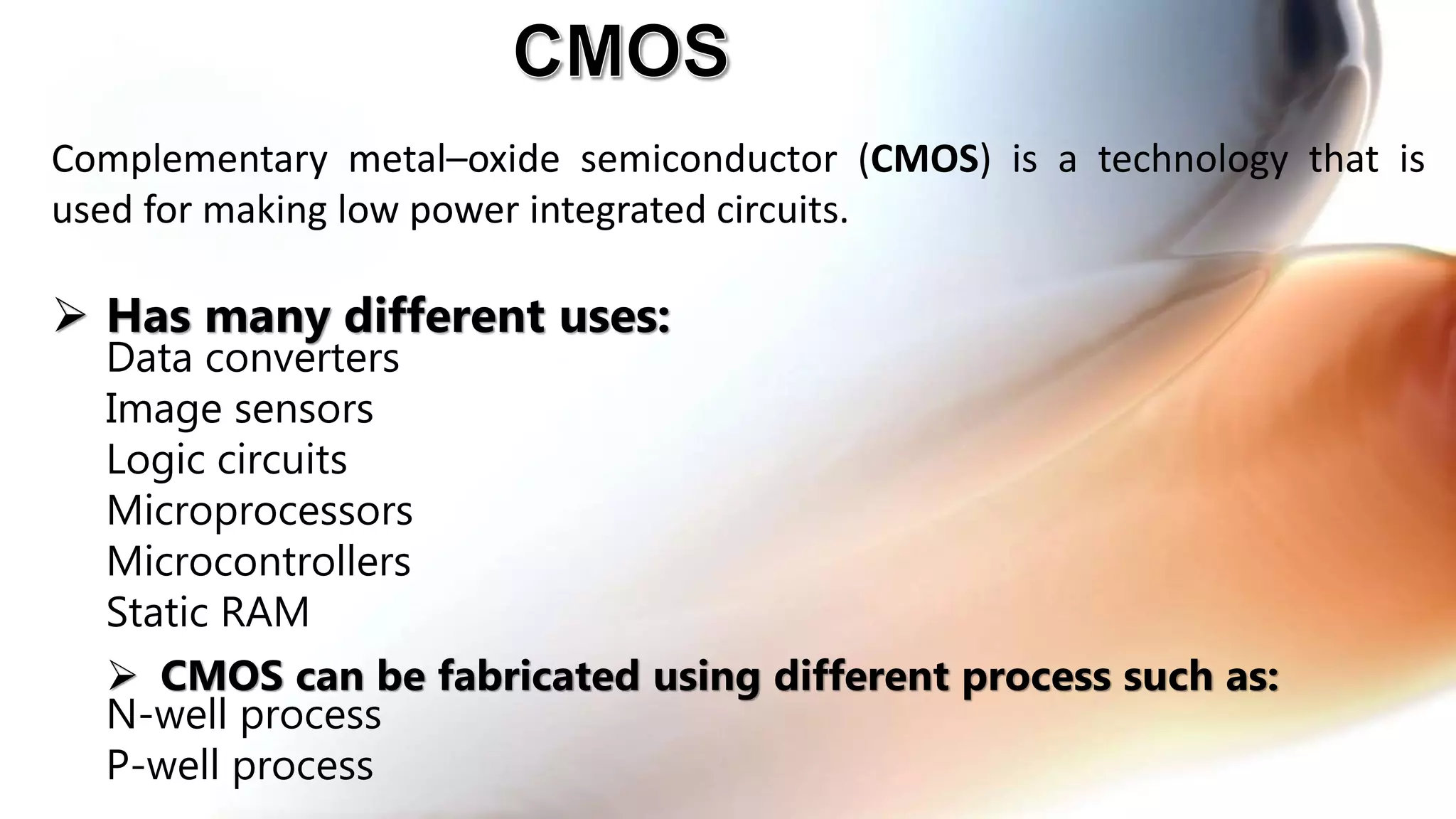
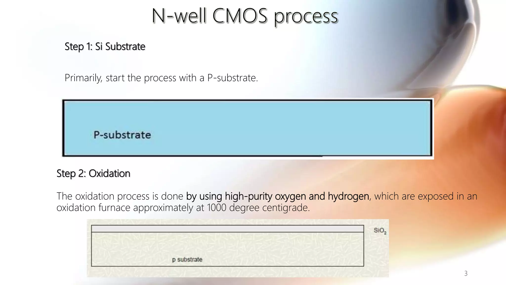
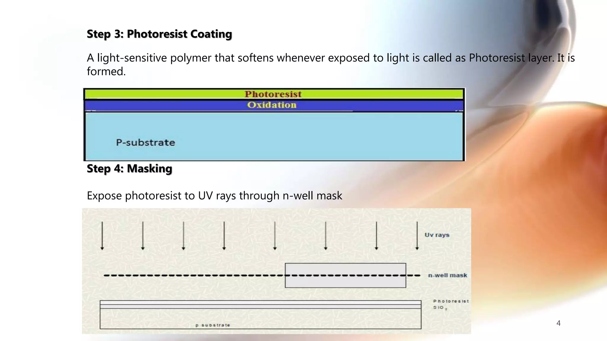
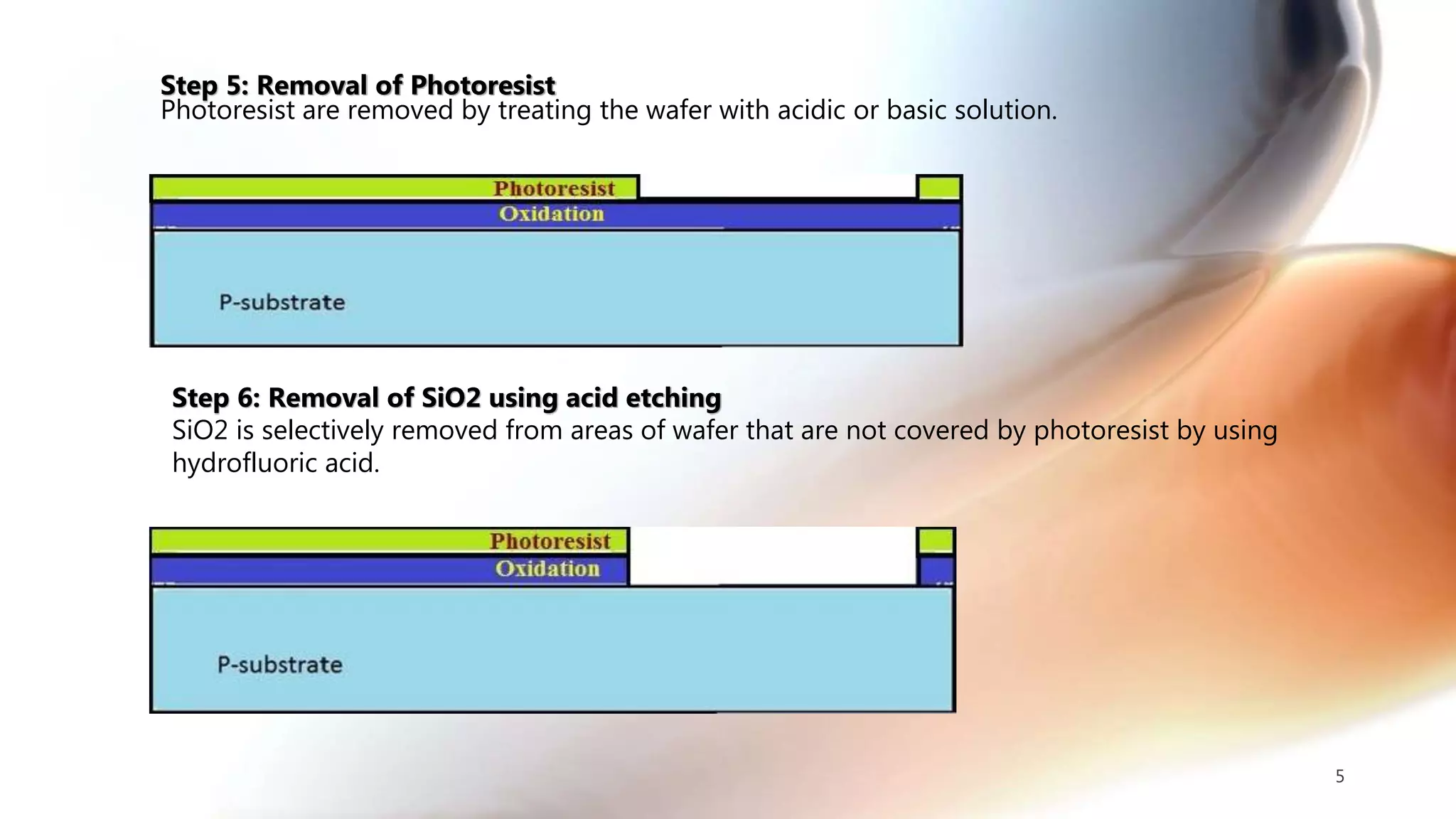
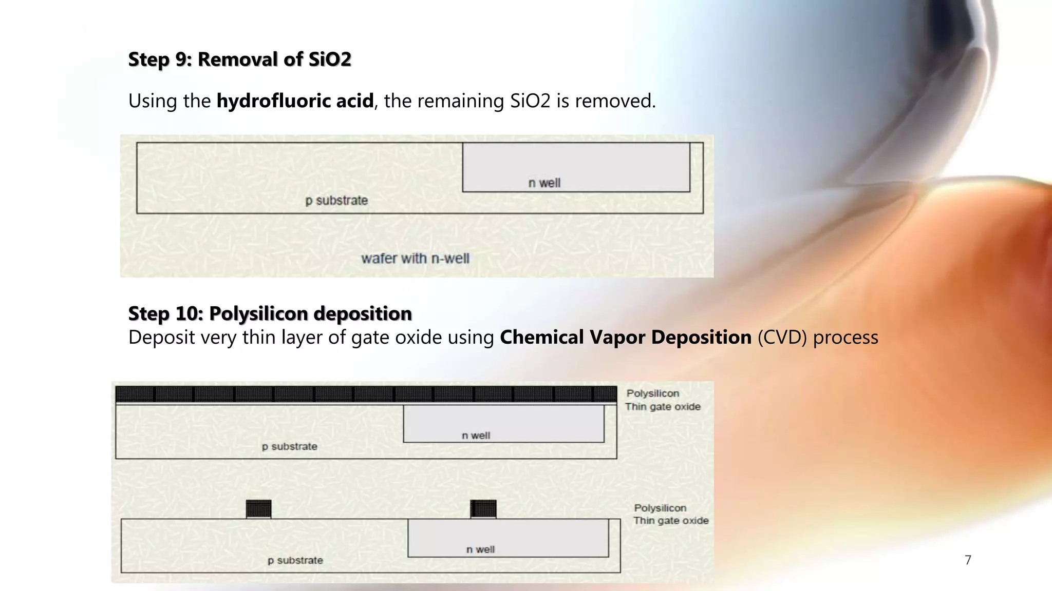
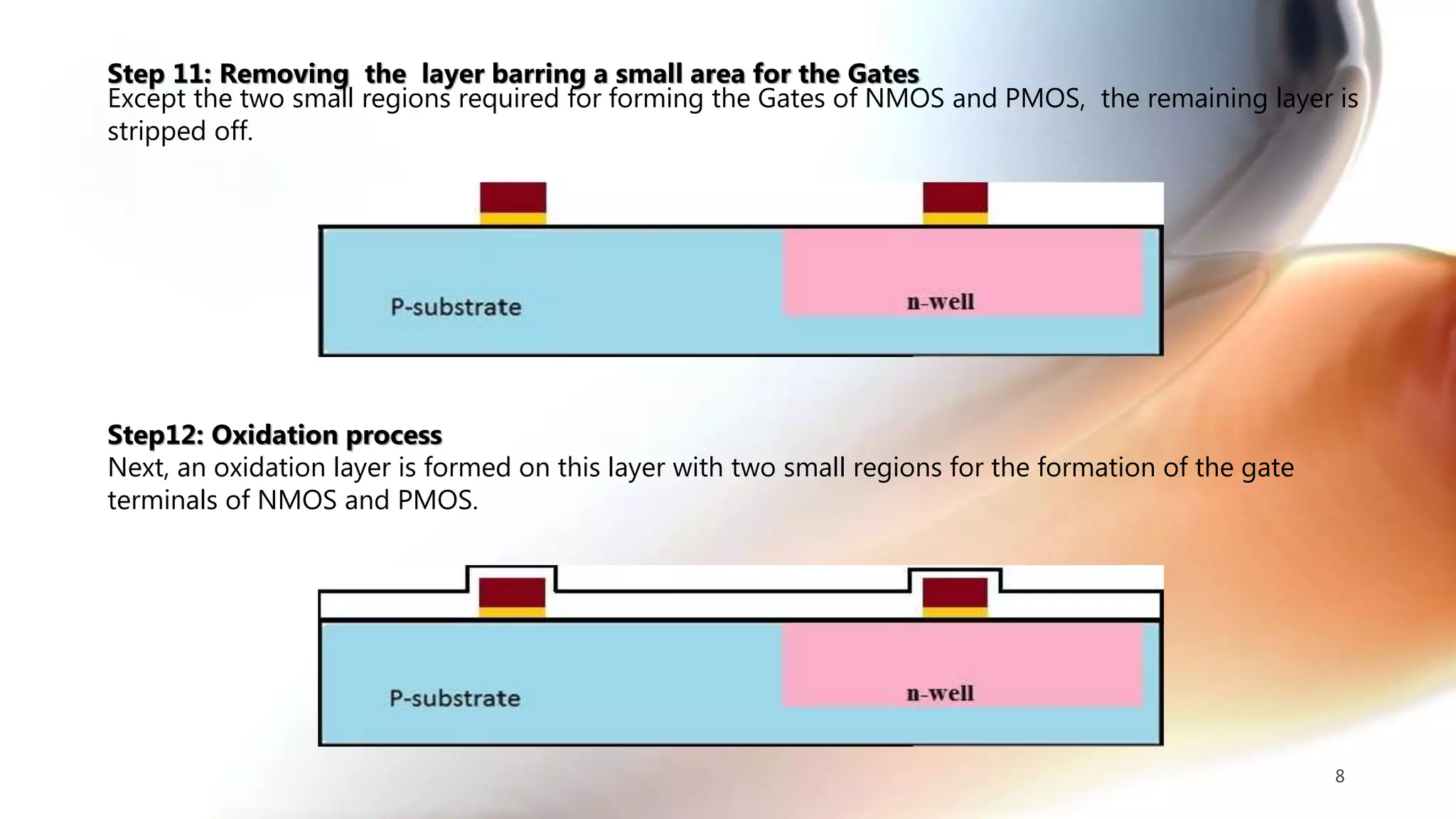
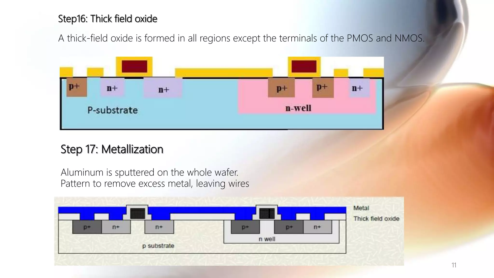
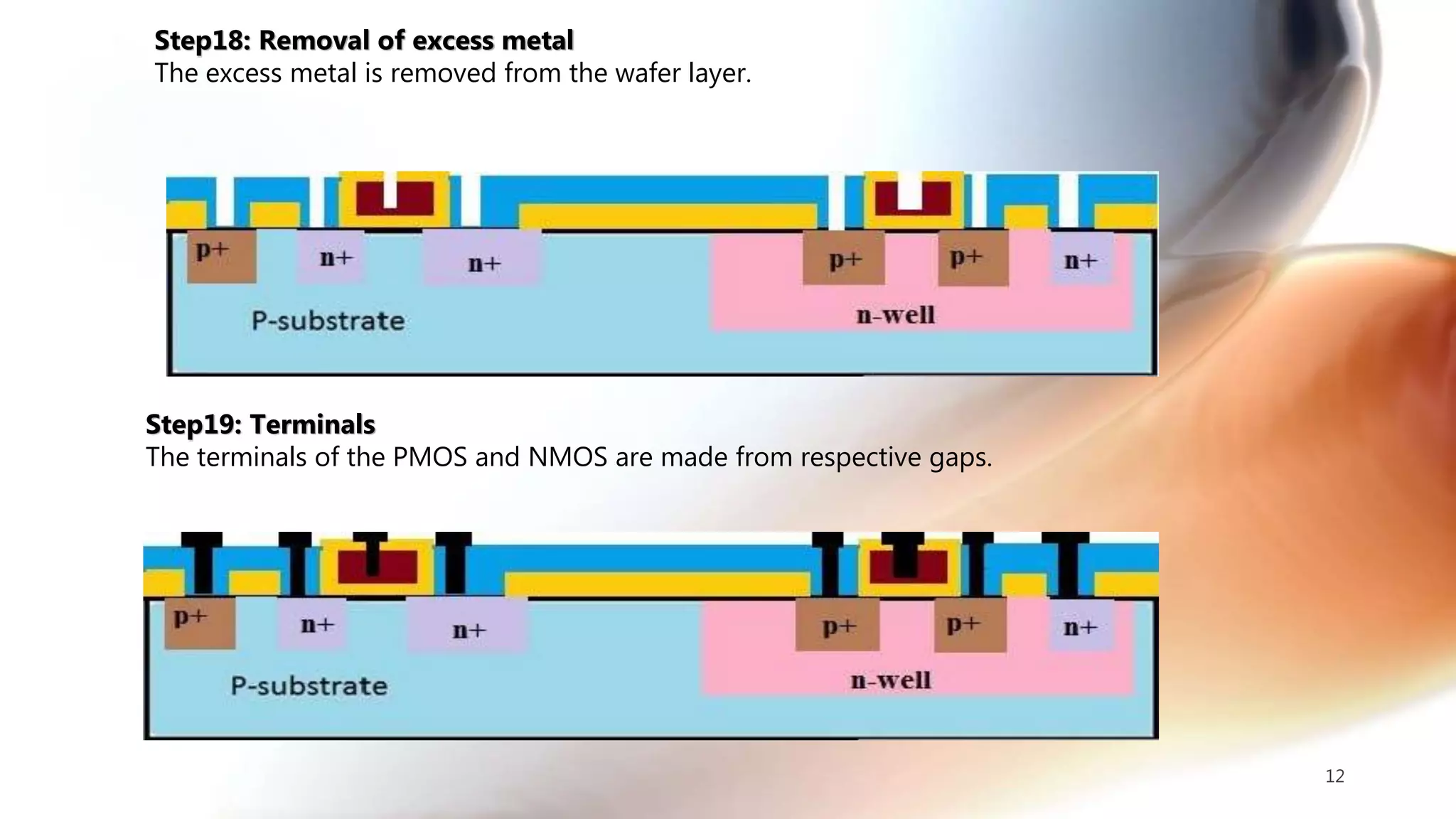
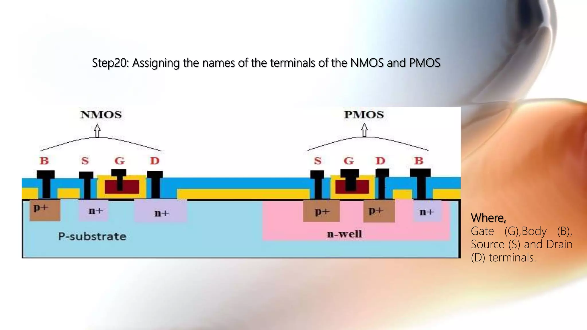
Name : Ananda Mohan Shil
ID : 15010324
Dept. : EEE
Batch : 15th
1
Complementary metal–oxide semiconductor (CMOS) is a technology that is
used for making low power integrated circuits.
 Has many different uses:
Data converters
Image sensors
Logic circuits
Microprocessors
Microcontrollers
Static RAM
 CMOS can be fabricated using different process such as:
N-well process
P-well process
Step 1: Si Substrate
Primarily, start the process with a P-substrate.
Step 2: Oxidation
The oxidation process is done by using high-purity oxygen and hydrogen, which are exposed in an
oxidation furnace approximately at 1000 degree centigrade.
3
Step 3: Photoresist Coating
A light-sensitive polymer that softens whenever exposed to light is called as Photoresist layer. It is
formed.
Step 4: Masking
Expose photoresist to UV rays through n-well mask
4
Step 5: Removal of Photoresist
Photoresist are removed by treating the wafer with acidic or basic solution.
Step 6: Removal of SiO2 using acid etching
SiO2 is selectively removed from areas of wafer that are not covered by photoresist by using
hydrofluoric acid.
5
Step 7: Removal of Photoresist
The entire photoresist layer is stripped off, as shown in the below figure.
Step 8: Formation of n-well
By using ion implantation or diffusion process N-well is formed.
6
Step 9: Removal of SiO2
Using the hydrofluoric acid, the remaining SiO2 is removed.
Step 10: Polysilicon deposition
Deposit very thin layer of gate oxide using Chemical Vapor Deposition (CVD) process
7
Step 11: Removing the layer barring a small area for the Gates
Except the two small regions required for forming the Gates of NMOS and PMOS, the remaining layer is
stripped off.
8
Step12: Oxidation process
Next, an oxidation layer is formed on this layer with two small regions for the formation of the gate
terminals of NMOS and PMOS.
Step13: Masking and N-diffusion
By using the masking process small gaps are made for the purpose of N-diffusion.
9
The n-type (n+) dopants are diffused or ion implanted, and the three n+ are formed for the
formation of the terminals of NMOS.
Step14: Oxide stripping
The remaining oxidation layer is stripped off.
Step15: P-diffusion
Similar to the above N-diffusion process, the P-diffusion regions are diffused to form
the terminals of the PMOS.
10
Step16: Thick field oxide
A thick-field oxide is formed in all regions except the terminals of the PMOS and NMOS.
11
Step 17: Metallization
Aluminum is sputtered on the whole wafer.
Pattern to remove excess metal, leaving wires
12
Step18: Removal of excess metal
The excess metal is removed from the wafer layer.
Step19: Terminals
The terminals of the PMOS and NMOS are made from respective gaps.
Step20: Assigning the names of the terminals of the NMOS and PMOS
Where,
Gate (G),Body (B),
Source (S) and Drain
(D) terminals.
Among all the fabrication processes of the CMOS, N-well process is mostly used for the fabrication of the
CMOS. P-well process is almost similar to the N-well. But the only difference in p-well process is that it consists
of a main N-substrate and, thus, P-wells itself acts as substrate for the N-devices.
14
Thank you
15

Cmos fabrication process

  • 1.
    Name : AnandaMohan Shil ID : 15010324 Dept. : EEE Batch : 15th 1
  • 2.
    Complementary metal–oxide semiconductor(CMOS) is a technology that is used for making low power integrated circuits.  Has many different uses: Data converters Image sensors Logic circuits Microprocessors Microcontrollers Static RAM  CMOS can be fabricated using different process such as: N-well process P-well process
  • 3.
    Step 1: SiSubstrate Primarily, start the process with a P-substrate. Step 2: Oxidation The oxidation process is done by using high-purity oxygen and hydrogen, which are exposed in an oxidation furnace approximately at 1000 degree centigrade. 3
  • 4.
    Step 3: PhotoresistCoating A light-sensitive polymer that softens whenever exposed to light is called as Photoresist layer. It is formed. Step 4: Masking Expose photoresist to UV rays through n-well mask 4
  • 5.
    Step 5: Removalof Photoresist Photoresist are removed by treating the wafer with acidic or basic solution. Step 6: Removal of SiO2 using acid etching SiO2 is selectively removed from areas of wafer that are not covered by photoresist by using hydrofluoric acid. 5
  • 6.
    Step 7: Removalof Photoresist The entire photoresist layer is stripped off, as shown in the below figure. Step 8: Formation of n-well By using ion implantation or diffusion process N-well is formed. 6
  • 7.
    Step 9: Removalof SiO2 Using the hydrofluoric acid, the remaining SiO2 is removed. Step 10: Polysilicon deposition Deposit very thin layer of gate oxide using Chemical Vapor Deposition (CVD) process 7
  • 8.
    Step 11: Removingthe layer barring a small area for the Gates Except the two small regions required for forming the Gates of NMOS and PMOS, the remaining layer is stripped off. 8 Step12: Oxidation process Next, an oxidation layer is formed on this layer with two small regions for the formation of the gate terminals of NMOS and PMOS.
  • 9.
    Step13: Masking andN-diffusion By using the masking process small gaps are made for the purpose of N-diffusion. 9 The n-type (n+) dopants are diffused or ion implanted, and the three n+ are formed for the formation of the terminals of NMOS.
  • 10.
    Step14: Oxide stripping Theremaining oxidation layer is stripped off. Step15: P-diffusion Similar to the above N-diffusion process, the P-diffusion regions are diffused to form the terminals of the PMOS. 10
  • 11.
    Step16: Thick fieldoxide A thick-field oxide is formed in all regions except the terminals of the PMOS and NMOS. 11 Step 17: Metallization Aluminum is sputtered on the whole wafer. Pattern to remove excess metal, leaving wires
  • 12.
    12 Step18: Removal ofexcess metal The excess metal is removed from the wafer layer. Step19: Terminals The terminals of the PMOS and NMOS are made from respective gaps.
  • 13.
    Step20: Assigning thenames of the terminals of the NMOS and PMOS Where, Gate (G),Body (B), Source (S) and Drain (D) terminals.
  • 14.
    Among all thefabrication processes of the CMOS, N-well process is mostly used for the fabrication of the CMOS. P-well process is almost similar to the N-well. But the only difference in p-well process is that it consists of a main N-substrate and, thus, P-wells itself acts as substrate for the N-devices. 14
  • 15.