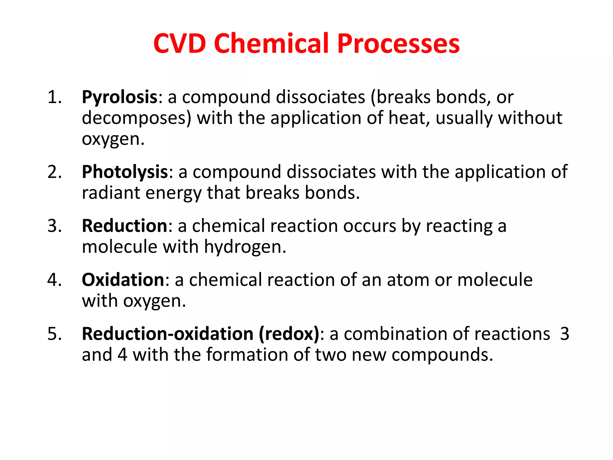
THIN FILMS
(Evaporation and Sputtering)
Dr. U P Singh
School of Electronics Engineering
Course Coverage
• Thin films :
• Physical deposition,
– Evaporation and sputtering ;
– Chemical Vapor Deposition techniques;
– Epitaxial growth
• Two main types of deposition methods have
been developed and are used in CMOS
technology:
• Physical Vapor Deposition (PVD)
- evaporation, sputter deposition
• Chemical Vapor Deposition (CVD)
- APCVD, LPCVD, PECVD, HDPCVD
• Many films, made of many different materials
are deposited during a standard CMOS
process.
• These layers include silicon dioxide, silicon
nitride, poly silicon and metal.
• In this set of notes we describe the
requirements, methods and equipment used
to deposit these thin films.
Film parameters
• Thickness/uniformity
• Surface flatness/roughness
• Composition/grain size
• Stress free
• Purity
• Integrity
Thin Film Characteristics
 Good step coverage
 Ability to fill high aspect ratio gaps (conformality)
 Good thickness uniformity
 High purity and density
 Controlled stoichiometries
 High degree of structural perfection with low film stress
 Good electrical properties
 Excellent adhesion to the substrate material and subsequent
films
Solid Thin Film
Silicon substrate
Oxide
Width
Thickness
Thin films are very thin in
comparison to the substrate.
Film Coverage over Steps
Conformal step coverage Nonconformal step coverage
Uniform thickness
Aspect Ratio for Film Deposition
Aspect Ratio =
Depth
Width
=
2
1
Aspect Ratio =
500 Å
250 Å
500
Å
D
250 Å
W
High Aspect Ratio Gap
Photograph courtesy of Integrated Circuit Engineering
Stages of Film Growth
Continuous film
Gas molecules
Nucleation Coalescenc
e
Substrate
Simple Evaporator
Roughing
pump
Hi-Vac valve
Hi-Vac pump
Process
chamber
(bell jar)
Crucible
Evaporating metal
Wafer carrier
Base pressure is as low as possible
• Heat the crucible to produce a vapor of
the charge material
• Vapor travels in a straight line to the
wafers producing a thin film
• Wafers positioned on a planetary for
uniformity
•In evaporation, source material is heated in high vacuum
chamber. (P <10-5 torr)
• Mostly line-of-sight deposition since pressure is low.
• Deposition rate is determined by emitted flux and by
geometry of the target.
The evaporation source can be considered either a point source or as a small
area surface source (latter is more applicable to most evaporation systems).
Simple Thermal Evaporator
Resistive evaporator sources
(A) Simple sources including heating the charge itself and using a coil of
refractory metal heater coil and a charge rod.
(B) More standard thermal sources including a dimpled boat in resistive
media.
 High deposition rate afforded by modern cathode and target design
 Capability to deposit and maintain complex alloy compositions
 Ability to deposit high-temperature and refractory metals
 Capability to maintain well-controlled, uniform deposition on large
(200 mm and larger) wafers
 Ability, in multi-chamber systems, to clean the contact before
depositing metal
• Sputtering is a term used to describe the mechanism
in which atoms are ejected from the surface of a
material when that surface is stuck by sufficiency
energetic particles.
• Alternative to evaporation.
• First discovered in 1852, and developed as a thin film
deposition technique by Langmuir in 1920.
• Metallic films: Al-alloys, Ti, TiW, TiN, Tantalum,
Nickel, Cobalt, Gold, etc.
• Sputtering is usually carried out in an argon
plasma and by biasing the target (source of
metal) negatively, argon ions are attracted to the
target
• The momentum of the Ar ions is transferred to
the target resulting in the ejection of one or more
atoms from the surface of the target
• The sputtered atoms, mostly neutral, fly into the
plasma and land on the wafer
• Like evaporation, sputter deposition occurs essentially along a
line-of-sight path with a cosine distribution
• Poor step coverage can result if the surface topography of the
wafer is abrupt
• The uniformity of the deposited film can be improved by raising
the substrate temperature (enhancing surface migration), using
a larger target, or inserting a collimator between the sputtering
cathode and wafer
• Better at depositing alloys and compounds than evaporation.
Reasons for sputtering
• Use large-area-targets which gives uniform
thickness over the wafer.
• Control the thickness by Dep. time and other
parameters.
• Control film properties such as step coverage
(negative bias), grain structure (wafer temp),
etc.
• Sputter-cleaned the surface in vacuum prior
to deposition.
Simple Parallel Plate DC Diode Sputtering System
Exhaust
e- e-
e-
DC diode
sputterer
Substrate
1) Electric
fields create
Ar+ ions.
2) High-energy
Ar+ ions collide
with metal target.
3) Metallic
atoms are
dislodged from
target.
Anode
(+)
Cathode
(-)
Argon
atoms
Electric field
Metal
target
Plasma
5) Metal deposits
on substrate
6) Excess matter is
removed from
chamber by a vacuum
pump.
4) Metal atoms migrate toward
substrate.
Gas delivery
+
+ + +
+
Dislodging Metal Atoms from Surface of
Sputtering Target
+
0
High-energy Ar+
ion
Sputtered
metal atom
Metal atoms
Cathode (-)
Rebounding argon ion
recombines with free
electron to form a neutral
atom.
• Rate of sputtering depends on the sputtering yield, S,
defined as the number of atoms or molecules ejected
from the target per incident ion.
• S is a function of the energy and mass of ions, and the
target material. It is also a function of incident angle.
• S does not vary between target materials as much as the
vapor pressure does.
• Yield vary from ~0.5-30, depending also on the
momentum of ion.
• Controlling composition of alloys is easier with sputtering
than with evaporation.
Step coverage
tends to be very
poor due to line-of-
sight deposition
process
•Heating allows
surface diffusion
and so improves
step coverage
•Generally only
acceptable for
aspect ratios of <
1:1
• Calculate the mean free path of a particle in the gas phase of a deposition system and
estimate the number of collisions it experiences in traveling from the source to the substrate
in each of the cases below. Assume that in each case the molecular collisional diameter is 0.4
nm, the source-to-substrate distance is 5 cm, and that the number of collisions is
approximately equal to the source-to-substrate distance divided by the mean free path.
a. An evaporation system in which the pressure is 10-5 torr and the temperature is 25°C.
b. A sputter deposition system in which the pressure is 3 mtorr and the temperature is 25°C
The mean free path of a gas particle λ = kT/2 πd2P
where k =1.36x10⁻²² cm3 atm K-1, T is the temperature in K, d is the collision diameter of the
molecule in cm (approximately 4x10⁻⁸ cm for most molecules of interest), and P is the pressure
in atm. The # collisions is approximately equal to the source-to substrate distance divided by
the mean free path in each case. Putting the values gives:
λ(in cm) = λ = kT/2 πd2P
= 1.36x10⁻²² cm3 ⋅ atm ⋅K−1 ∗ T(K) /  2π(4x10⁻⁸ cm)2 P(torr) /760torr / atm
= 1.45x10⁻⁵ T(K) /P(torr)
a. 433 cm, 1.2x10⁻² collisions;
b. 1.44 cm, 3.5 collisions;
Chemical Vapor Deposition
•Excellent step coverage
•Large throughput
•Low-temperature processing
•A number of metals and metal compounds, such as Al, Cu,
WSi2, TiN, and W, can be deposited by chemical reaction or
thermal decomposition of precursors
•Usually the wafer needs to be heated to 100oC to 800oC to
provide the initial thermal energy to overcome the reaction
barrier
Chemical Vapor Deposition
The Essential Aspects of CVD
1. Chemical action is involved, either through chemical
reaction or by thermal decomposition (referred to as
pyrolysis).
2. All material for the thin film is supplied by an external
source.
3. The reactants in a CVD process must start out in the vapor
phase (as a gas).
Chemical Vapor Deposition (CVD)
- APCVD (Atm pressure CVD),
- LPCVD, (Low Pressure CVD)
- PECVD, (Plasma Enhanced CVD)
- HDPCVD, (High Density Plasma CVD)
CVD Chemical Processes
1. Pyrolosis: a compound dissociates (breaks bonds, or
decomposes) with the application of heat, usually without
oxygen.
2. Photolysis: a compound dissociates with the application of
radiant energy that breaks bonds.
3. Reduction: a chemical reaction occurs by reacting a
molecule with hydrogen.
4. Oxidation: a chemical reaction of an atom or molecule
with oxygen.
5. Reduction-oxidation (redox): a combination of reactions 3
and 4 with the formation of two new compounds.
A simple CVD reactor
Steps involved in a CVD process:
1. Transport of reactants to the deposition region.
2. Transport of reactants from the main gas stream through the
boundary layer to the wafer surface.
3. Adsorption of reactants on the wafer surface.
4. Surface reactions, including: chemical decomposition or
reaction, surface migration to attachment sites (kinks and
ledges); site incorporation; and other surface reactions
(emission and re-deposition for example).
5. Desorption or reemission of by-products.
6. Transport of by-products through the boundary layer.
7. Transport of by-products away from the deposition region.
Epitaxy
• Epitaxy Growth Model
• Epitaxy Growth Methods
– Vapor-Phase Epitaxy (VPE)
– Metalorganic CVD (MOCVD)
– Molecular-Beam Epitaxy (MBE)
Epitaxy is the process of the controlled growth of a crystalline doped layer of
silicon on a single crystal substrate.
Silicon Epitaxial Growth on a Silicon
Wafer
Si
Si
Cl
Cl
H
H
Si
Si
Si Si
Si Si
Si
Si
Si
Si
Si
Cl
H
Cl
H
Chemical reaction
By-products
Deposited silicon
Epitaxial layer
Single silicon substrate
Illustration of Vapor Phase Epitaxy
Dopant
(AsH3 or B2 H3)
H2
SiH2 Cl2
RF induction-heating coils
Susceptor
Wafers
Vacuum
puimp
Silicon Vapor Phase Epitaxy Reactors
Exhaust
Exhaust
Exhaust
RF heating
RF heating
Gas inlet
Gas inlet
Horizontal
reactor
Barrel reactor
Vertical reactor
Effects of Keyholes in ILD on Metal Step Coverage
b) SiO2 is planarized
c) Next layer of aluminum is deposited
Metal void caused by keyhole defect in SiO2
a) SiO2 deposited by PECVD
SiO2
Keyhole defect in
interlayer dielectric
Aluminum
ILD: Interlayer Dielectric
THIN FILMS.pdf
THIN FILMS.pdf

THIN FILMS.pdf

  • 1.
    THIN FILMS (Evaporation andSputtering) Dr. U P Singh School of Electronics Engineering
  • 2.
    Course Coverage • Thinfilms : • Physical deposition, – Evaporation and sputtering ; – Chemical Vapor Deposition techniques; – Epitaxial growth
  • 3.
    • Two maintypes of deposition methods have been developed and are used in CMOS technology: • Physical Vapor Deposition (PVD) - evaporation, sputter deposition • Chemical Vapor Deposition (CVD) - APCVD, LPCVD, PECVD, HDPCVD
  • 4.
    • Many films,made of many different materials are deposited during a standard CMOS process. • These layers include silicon dioxide, silicon nitride, poly silicon and metal. • In this set of notes we describe the requirements, methods and equipment used to deposit these thin films.
  • 5.
    Film parameters • Thickness/uniformity •Surface flatness/roughness • Composition/grain size • Stress free • Purity • Integrity
  • 6.
    Thin Film Characteristics Good step coverage  Ability to fill high aspect ratio gaps (conformality)  Good thickness uniformity  High purity and density  Controlled stoichiometries  High degree of structural perfection with low film stress  Good electrical properties  Excellent adhesion to the substrate material and subsequent films
  • 7.
    Solid Thin Film Siliconsubstrate Oxide Width Thickness Thin films are very thin in comparison to the substrate.
  • 8.
    Film Coverage overSteps Conformal step coverage Nonconformal step coverage Uniform thickness
  • 9.
    Aspect Ratio forFilm Deposition Aspect Ratio = Depth Width = 2 1 Aspect Ratio = 500 Å 250 Å 500 Å D 250 Å W
  • 10.
    High Aspect RatioGap Photograph courtesy of Integrated Circuit Engineering
  • 11.
    Stages of FilmGrowth Continuous film Gas molecules Nucleation Coalescenc e Substrate
  • 13.
    Simple Evaporator Roughing pump Hi-Vac valve Hi-Vacpump Process chamber (bell jar) Crucible Evaporating metal Wafer carrier Base pressure is as low as possible • Heat the crucible to produce a vapor of the charge material • Vapor travels in a straight line to the wafers producing a thin film • Wafers positioned on a planetary for uniformity
  • 14.
    •In evaporation, sourcematerial is heated in high vacuum chamber. (P <10-5 torr) • Mostly line-of-sight deposition since pressure is low. • Deposition rate is determined by emitted flux and by geometry of the target. The evaporation source can be considered either a point source or as a small area surface source (latter is more applicable to most evaporation systems).
  • 15.
    Simple Thermal Evaporator Resistiveevaporator sources (A) Simple sources including heating the charge itself and using a coil of refractory metal heater coil and a charge rod. (B) More standard thermal sources including a dimpled boat in resistive media.
  • 17.
     High depositionrate afforded by modern cathode and target design  Capability to deposit and maintain complex alloy compositions  Ability to deposit high-temperature and refractory metals  Capability to maintain well-controlled, uniform deposition on large (200 mm and larger) wafers  Ability, in multi-chamber systems, to clean the contact before depositing metal
  • 18.
    • Sputtering isa term used to describe the mechanism in which atoms are ejected from the surface of a material when that surface is stuck by sufficiency energetic particles. • Alternative to evaporation. • First discovered in 1852, and developed as a thin film deposition technique by Langmuir in 1920. • Metallic films: Al-alloys, Ti, TiW, TiN, Tantalum, Nickel, Cobalt, Gold, etc.
  • 19.
    • Sputtering isusually carried out in an argon plasma and by biasing the target (source of metal) negatively, argon ions are attracted to the target • The momentum of the Ar ions is transferred to the target resulting in the ejection of one or more atoms from the surface of the target • The sputtered atoms, mostly neutral, fly into the plasma and land on the wafer
  • 20.
    • Like evaporation,sputter deposition occurs essentially along a line-of-sight path with a cosine distribution • Poor step coverage can result if the surface topography of the wafer is abrupt • The uniformity of the deposited film can be improved by raising the substrate temperature (enhancing surface migration), using a larger target, or inserting a collimator between the sputtering cathode and wafer • Better at depositing alloys and compounds than evaporation.
  • 21.
    Reasons for sputtering •Use large-area-targets which gives uniform thickness over the wafer. • Control the thickness by Dep. time and other parameters. • Control film properties such as step coverage (negative bias), grain structure (wafer temp), etc. • Sputter-cleaned the surface in vacuum prior to deposition.
  • 23.
    Simple Parallel PlateDC Diode Sputtering System Exhaust e- e- e- DC diode sputterer Substrate 1) Electric fields create Ar+ ions. 2) High-energy Ar+ ions collide with metal target. 3) Metallic atoms are dislodged from target. Anode (+) Cathode (-) Argon atoms Electric field Metal target Plasma 5) Metal deposits on substrate 6) Excess matter is removed from chamber by a vacuum pump. 4) Metal atoms migrate toward substrate. Gas delivery + + + + +
  • 24.
    Dislodging Metal Atomsfrom Surface of Sputtering Target + 0 High-energy Ar+ ion Sputtered metal atom Metal atoms Cathode (-) Rebounding argon ion recombines with free electron to form a neutral atom.
  • 25.
    • Rate ofsputtering depends on the sputtering yield, S, defined as the number of atoms or molecules ejected from the target per incident ion. • S is a function of the energy and mass of ions, and the target material. It is also a function of incident angle. • S does not vary between target materials as much as the vapor pressure does. • Yield vary from ~0.5-30, depending also on the momentum of ion. • Controlling composition of alloys is easier with sputtering than with evaporation.
  • 28.
    Step coverage tends tobe very poor due to line-of- sight deposition process •Heating allows surface diffusion and so improves step coverage •Generally only acceptable for aspect ratios of < 1:1
  • 31.
    • Calculate themean free path of a particle in the gas phase of a deposition system and estimate the number of collisions it experiences in traveling from the source to the substrate in each of the cases below. Assume that in each case the molecular collisional diameter is 0.4 nm, the source-to-substrate distance is 5 cm, and that the number of collisions is approximately equal to the source-to-substrate distance divided by the mean free path. a. An evaporation system in which the pressure is 10-5 torr and the temperature is 25°C. b. A sputter deposition system in which the pressure is 3 mtorr and the temperature is 25°C The mean free path of a gas particle λ = kT/2 πd2P where k =1.36x10⁻²² cm3 atm K-1, T is the temperature in K, d is the collision diameter of the molecule in cm (approximately 4x10⁻⁸ cm for most molecules of interest), and P is the pressure in atm. The # collisions is approximately equal to the source-to substrate distance divided by the mean free path in each case. Putting the values gives: λ(in cm) = λ = kT/2 πd2P = 1.36x10⁻²² cm3 ⋅ atm ⋅K−1 ∗ T(K) /  2π(4x10⁻⁸ cm)2 P(torr) /760torr / atm = 1.45x10⁻⁵ T(K) /P(torr) a. 433 cm, 1.2x10⁻² collisions; b. 1.44 cm, 3.5 collisions;
  • 32.
    Chemical Vapor Deposition •Excellentstep coverage •Large throughput •Low-temperature processing •A number of metals and metal compounds, such as Al, Cu, WSi2, TiN, and W, can be deposited by chemical reaction or thermal decomposition of precursors •Usually the wafer needs to be heated to 100oC to 800oC to provide the initial thermal energy to overcome the reaction barrier
  • 33.
    Chemical Vapor Deposition TheEssential Aspects of CVD 1. Chemical action is involved, either through chemical reaction or by thermal decomposition (referred to as pyrolysis). 2. All material for the thin film is supplied by an external source. 3. The reactants in a CVD process must start out in the vapor phase (as a gas). Chemical Vapor Deposition (CVD) - APCVD (Atm pressure CVD), - LPCVD, (Low Pressure CVD) - PECVD, (Plasma Enhanced CVD) - HDPCVD, (High Density Plasma CVD)
  • 34.
    CVD Chemical Processes 1.Pyrolosis: a compound dissociates (breaks bonds, or decomposes) with the application of heat, usually without oxygen. 2. Photolysis: a compound dissociates with the application of radiant energy that breaks bonds. 3. Reduction: a chemical reaction occurs by reacting a molecule with hydrogen. 4. Oxidation: a chemical reaction of an atom or molecule with oxygen. 5. Reduction-oxidation (redox): a combination of reactions 3 and 4 with the formation of two new compounds.
  • 35.
    A simple CVDreactor
  • 39.
    Steps involved ina CVD process: 1. Transport of reactants to the deposition region. 2. Transport of reactants from the main gas stream through the boundary layer to the wafer surface. 3. Adsorption of reactants on the wafer surface. 4. Surface reactions, including: chemical decomposition or reaction, surface migration to attachment sites (kinks and ledges); site incorporation; and other surface reactions (emission and re-deposition for example). 5. Desorption or reemission of by-products. 6. Transport of by-products through the boundary layer. 7. Transport of by-products away from the deposition region.
  • 42.
    Epitaxy • Epitaxy GrowthModel • Epitaxy Growth Methods – Vapor-Phase Epitaxy (VPE) – Metalorganic CVD (MOCVD) – Molecular-Beam Epitaxy (MBE) Epitaxy is the process of the controlled growth of a crystalline doped layer of silicon on a single crystal substrate.
  • 46.
    Silicon Epitaxial Growthon a Silicon Wafer Si Si Cl Cl H H Si Si Si Si Si Si Si Si Si Si Si Cl H Cl H Chemical reaction By-products Deposited silicon Epitaxial layer Single silicon substrate
  • 47.
    Illustration of VaporPhase Epitaxy Dopant (AsH3 or B2 H3) H2 SiH2 Cl2 RF induction-heating coils Susceptor Wafers Vacuum puimp
  • 48.
    Silicon Vapor PhaseEpitaxy Reactors Exhaust Exhaust Exhaust RF heating RF heating Gas inlet Gas inlet Horizontal reactor Barrel reactor Vertical reactor
  • 49.
    Effects of Keyholesin ILD on Metal Step Coverage b) SiO2 is planarized c) Next layer of aluminum is deposited Metal void caused by keyhole defect in SiO2 a) SiO2 deposited by PECVD SiO2 Keyhole defect in interlayer dielectric Aluminum ILD: Interlayer Dielectric