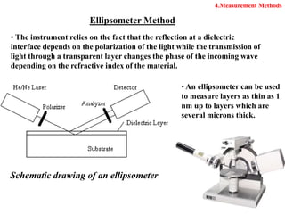
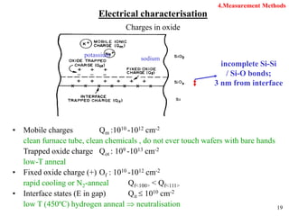
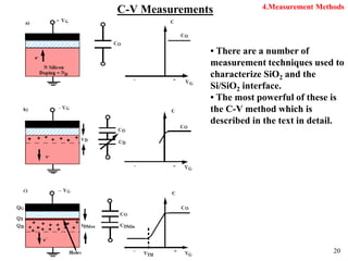
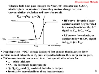
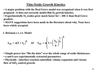
Chapter 6: Thermal Oxidation and the Si/SiO2
Interface
2
Contents
1. Introduction
2. Structure
3. Manufacturing Methods and Equipment
4. Measurement Methods
5. Growth kinetics
– Deal Grove model
– Influence ambient
6. Trends
7. Summarisation
3
Thermally grown oxides:
• Si is unique, its oxide (SiO2) and the Si/SiO2 interface
are very stable.
Nothing in this world is perfect:
• When SiO2 is formed, misfit at the interface causes
interface states and some Si atoms in the SiO2 near the
interface are positively ionised (fixed oxide charge)=>
shift in MOST Vt (threshold voltage).
• Sodium (Na) and Potasium (K) are incorporated and
form mobile ions => instabilities of MOST Vt
1. Introduction
4
1. Introduction
Thermal oxides are used for:
• Gate oxide 2-10 nm
Dry oxidation (slow) Si + O2 => SiO2
• Pad oxide (20 nm, dry) between Si3N4 and Si for LOCOS (LOCal
Oxidation of Silicon)
• Electrical isolation between devices (lateral);
Field Oxide (0.5-1 mm)
Wet oxidation (fast) Si+2H2O => SiO2+2H2
• Masking layers (0.5-1.0 mm wet) for implantation and diffusion of
doping atoms
• The dielectric between conductors and the protection on top are
made by CVD (Chemical Vapor Deposition)
5
3. Structure
• tetrahedron
• amorphous
• no periodic structure of lattice, density low 
diffusion rel. easy
• quartzite: crystalline structure
6
• diffusion of oxidant through already grown SiO2-layer
• at Si-SiO2 interface: reaction of oxidant with Si
thickness SiO2 = x 
consumed Si-thickness = 0.44x
2
2
2
2
2
2
2 H
SiO
O
H
Si
SiO
O
Si





7
mole
cm
cm
g
mole
g
/
18
.
27
/
21
.
2
/
08
.
60 3
2

volume of 1 mole of Si =
• volume of 1 mole of SiO2 =
• 1 mole SiO2 uses 1 mole of Si
• To grow 100 Å thick SiO2, 44 Å Si is consumed
density
weight
molecular
mole
of
volume 
1
mole
cm
cm
g
mole
g
/
06
.
12
/
33
.
2
/
09
.
28 3
3

area
thickness
volume 

44
.
0
18
.
27
06
.
12
2


SiO
Si
h
h
8
Field oxide - LOCOS
• Lateral isolation between devices
• Thick : Wet oxidation
• LOCOS: Local oxidation of Silicon
• bird's beak!
Fully recessed LOCOS:
prior to oxidation
etch trench in Silicon
Pad oxide
9
Field Oxide - Shallow Trench Isolation
+ Less area loss ( higher packing density)
+ planar surface
+ easy downscaling
Trenches, reoxidation + B-implant, CVD oxide + CMP,
spacers, etching pad oxide, gate -oxidation + -deposition
10
3. Manufacturing Methods and Equipment
Oxidation Techniques
• Thermal Oxidation
• Rapid Thermal Oxidation
Thermal Oxidation Techniques
• Wet Oxidation
Si (solid) + H20 => SiO2 (solid) + 2H2
• Dry Oxidation
Si (solid) + O2 (gas) => SiO2(solid)
11
3. Manufacturing Methods and Equipment
Furnace:
Temperature: 700C - 1200C
Ambient: oxygen ("dry oxidation")
water vapour or burning hydrogen flame ("wet oxidation")
12
Wafers are placed in wafer load station
• Dry nitrogen is introduced into chamber
- Nitrogen prevents oxidation from occurring
• Nitrogen gas flow shut off and oxygen added to chamber
- Occurs when furnace has reached maximum temperature
- Oxygen can be in a dry gas or in a water vapor state
• Nitrogen gas reintroduced into chamber
- Stops oxidation process
• Wafers are removed from furnace and inspected
Dry Thermal Oxidation Characteristics
• Oxidant is dry oxygen
• Used to grow oxides less than 1000Å thick
• Slow process
- 140 - 250Å / hour
13
Thin Oxide Growth
• Thin oxides grown (<150Å) for features smaller than 1mm
- MOS transistors, MOS gates, and dielectric components
• Additional of chemical species to oxygen decreases oxide
growth rate (only in special cases)
- Hydrochloric acid (HCI)
- Trichloroethylene (TCE)
- Trichloroethane (TCA)
• Decreasing pressure slows down oxide growth rate
14
Wet Thermal Oxidation Characteristics
• Oxidant is water vapor
• Fast oxidation rate
- Oxide growth rate is 1000-1200Å / hour
• Preferred oxidation process for growth of thick oxides
15
Oxidation occurs in tube furnace
- Vertical Tube Furnace
- Horizontal Tube Furnace
Modern Equipments
16
4.Measurement Methods
Physical Measurements
Step measurements:
--step
-SEM
-AFM
-TEM
Si
SiO2
TEM image
Si
SiO2
SEM image
17
Optical Characterisation
n1/n0 = sinf/sinb > lmin,max = 2 n1x0 cosb/m
m= 1,2,3… for maximum, 0.5, 1.5, 2.5… for minimum
4.Measurement Methods
18
Schematic drawing of an ellipsometer
• The instrument relies on the fact that the reflection at a dielectric
interface depends on the polarization of the light while the transmission of
light through a transparent layer changes the phase of the incoming wave
depending on the refractive index of the material.
Ellipsometer Method
• An ellipsometer can be used
to measure layers as thin as 1
nm up to layers which are
several microns thick.
4.Measurement Methods
19
Electrical characterisation
Charges in oxide
• Mobile charges Qm :1010 -1012 cm-2
clean furnace tube, clean chemicals , do not ever touch wafers with bare hands
Trapped oxide charge Qot : 109 -1013 cm-2
low-T anneal
• Fixed oxide charge (+) Of : 1010 -1012 cm-2
rapid cooling or N2-anneal Qf<100> < Qf<111>
• Interface states (E in gap) Qit  1010 cm-2
low T (450ºC) hydrogen anneal  neutralisation
potassium
sodium
incomplete Si-Si
/ Si-O bonds;
3 nm from interface
4.Measurement Methods
20
C-V Measurements
• There are a number of
measurement techniques used to
characterize SiO2 and the
Si/SiO2 interface.
• The most powerful of these is
the C-V method which is
described in the text in detail.
4.Measurement Methods
21
• Electric field lines pass through the “perfect” insulator and Si/SiO2
interface, into the substrate where they control charge carriers.
• Accumulation, depletion and inversion result.
• HF curve - inversion layer
carriers cannot be generated
fast enough to follow the AC
signal so Cinv is Cox + CD
• LF curve - inversion layer
carriers follow the AC signal
so Cinv is just Cox.
• Deep depletion - “DC” voltage is applied fast enough that inversion layer
carriers cannot follow it, so CD must expand to balance the charge on the gate.
• C-V measurements can be used to extract quantitative values for:
• tox - oxide thickness
• NA - the substrate doping profile
• Qf, Qit, Qm, and Qot - oxide & interface charges.
• See text for more details on these measurements.
4.Measurement Methods
22
5. Growth kinetics
Deal-Grove model
• The basic model for oxidation was developed in 1965 by Deal and Grove.
Si+O2 => SiO2
Si+2H2O => SiO2+2H2 )
• Three first order flux equations describe the three series parts of the process.
23
5. Growth kinetics
• Three first order flux equations
describe the three series parts of
the process.
• Under steady state conditions,
F1 = F2 = F3, so
• Note that the simplifications are
made by neglecting F1 which is a
very good approximation.
• Combining (3) and (4), we have
(4)
(5)
(1)
(2)
(3)
(6)
24
• Integrating this equation (6) (see text), results in the
linear parabolic model.
Where ( parabolic rate constant)
(linear rate constant)
(7)
• (7) can also be written with oxide thickness as a function of time.
where
t>>A2/4B (long time)
xo
2=B(t+τ) Parabolic rate
t+ τ <<A2/4B (short time)
xo=(B/A)(t+τ) Linear rate
25
• The rate constants B and B/A have physical meaning (oxidant diffusion and
interface reaction rate respectively).
26
27
• Calculated dry O2 oxidation rates using Deal Grove.
28
• Calculated H2O oxidation rates using Deal Grove.
29
Thin Oxide Growth Kinetics
• A major problem with the Deal Grove model was recognized when it was first
proposed - it does not correctly model thin O2 growth kinetics.
• Experimentally O2 oxides grow much faster for ~ 200 Å than Deal Grove
predicts.
• MANY suggestions have been made in the literature about why. None have
been widely accepted.
1. Reisman e t. a l. Model
• Simple power law “fits the data” over the whole range of oxide thicknesses.
• a and b are experimentally extracted parameters.
• Physically - interface reaction controlled, volume expansion and viscous
flow of SiO2 control growth.
30
2. Han and Helms Model
• Second parallel reaction added - “fits the data” ” over the whole range
of oxide thicknesses.
• Three parameters (one of the A values is 0).
• Physically - second process may be outdiffusion of OV and reaction at
the gas/SiO2 interface.
3. M assoud e t. a l. Model
• Second term added to Deal Grove model which gives a higher dx/dt during
initial growth.
• L ~ 70 Å so the second term disappears for thicker oxides.
• Because it is simply implemented along with the Deal
Grove model, this model has been used in process simulators.
• Experimental data agrees with the Reisman, Han and Massoud models. (800°C
dry O2 model comparison below.)
31
32
Pressure Dependence
B and B/A  C0 and thus also  P :
P   growth rate 
 enables oxide growth at lower
temperatures
O
H
for
P
B
B
P
B
A
B
A i
i
2
)
(








O
for
P
B
B
P
B
A
B
A i
n
i
2
)
(








33
Dependence on Si Substrate Orientation
Wafer Orientation
• Oxide grows faster on <111>
wafers
- more silicon atoms available
to react with oxidant
• Affects oxide growth rate during
Linear Stage
34
Influence of impurities
• H2O impurity in O2-gas: hydroxyl groups are formed 
more open oxide structure  R
• HCl gas: is able to react with impurities and form
volatile chlorides
 quality of oxide and Si-SiO2 interface improves
• high concentrations of P and B change fermi level and
vacancy concentration:
– B segregates into oxide 
weakens the Si-O2 bond 
enlarges the diffusion
– P segregates into Si 
surface concentration of P 
B/A
35
Influence Halogens (Chlorine)
increase of growth rate
0-5% HCl
Is often added to improve gate oxide quality
36
Oxidation of doped Si
Boron
doped
Si
Phosphorus
doped
Si
37
2D SiO2 Growth Kinetics
• 950 °C oxidation (left), 1100 °C oxidation right
38
• These effects were investigated in detail experimentally by Kao et. al. about
10 years ago.
• Typical experimental
results (from Kao et.al.)
39
Trends
• Improve Si/SiO2 interface properties
– non-stoichometric monolayer due to incomplete oxidation - dangling
bonds
– strained region (1-4 nm) due to lattice mismatch
Solve by
– Fluorine incorporation (Si-F)
– Nitridation of oxides N2O, NH3 (Si-N)
Further: Si-N: improved barrier to B penetration
Optimum: N2O; 0.5 - 1 at% N at interface
• Ultra thin dielectrics
down to 2 nm (<0.1 mm MOS)
• Deposited gate dielectrics (less strain, less defects)
• Ultra clean technology (reduce defect density)
• Cluster tools (more clean process)
40
Summarisation
• Furnace oxidation is very well controlled process and is
widely used in IC fabrication
• Model of Deal-Grove widely accepted, except for thin oxide
growth in dry O2
• Oxide growth rate depends on crystal orientation, mechanical
stress, ambient (dry, wet, pressure, impurities, …)
• Si(100) most used material
• LOCOS - STI
• Electrical characterisation of quality of oxide
• Trends to improve quality

Chapter5_Oxidation.ppt

  • 1.
    Chapter 6: ThermalOxidation and the Si/SiO2 Interface
  • 2.
    2 Contents 1. Introduction 2. Structure 3.Manufacturing Methods and Equipment 4. Measurement Methods 5. Growth kinetics – Deal Grove model – Influence ambient 6. Trends 7. Summarisation
  • 3.
    3 Thermally grown oxides: •Si is unique, its oxide (SiO2) and the Si/SiO2 interface are very stable. Nothing in this world is perfect: • When SiO2 is formed, misfit at the interface causes interface states and some Si atoms in the SiO2 near the interface are positively ionised (fixed oxide charge)=> shift in MOST Vt (threshold voltage). • Sodium (Na) and Potasium (K) are incorporated and form mobile ions => instabilities of MOST Vt 1. Introduction
  • 4.
    4 1. Introduction Thermal oxidesare used for: • Gate oxide 2-10 nm Dry oxidation (slow) Si + O2 => SiO2 • Pad oxide (20 nm, dry) between Si3N4 and Si for LOCOS (LOCal Oxidation of Silicon) • Electrical isolation between devices (lateral); Field Oxide (0.5-1 mm) Wet oxidation (fast) Si+2H2O => SiO2+2H2 • Masking layers (0.5-1.0 mm wet) for implantation and diffusion of doping atoms • The dielectric between conductors and the protection on top are made by CVD (Chemical Vapor Deposition)
  • 5.
    5 3. Structure • tetrahedron •amorphous • no periodic structure of lattice, density low  diffusion rel. easy • quartzite: crystalline structure
  • 6.
    6 • diffusion ofoxidant through already grown SiO2-layer • at Si-SiO2 interface: reaction of oxidant with Si thickness SiO2 = x  consumed Si-thickness = 0.44x 2 2 2 2 2 2 2 H SiO O H Si SiO O Si     
  • 7.
    7 mole cm cm g mole g / 18 . 27 / 21 . 2 / 08 . 60 3 2  volume of1 mole of Si = • volume of 1 mole of SiO2 = • 1 mole SiO2 uses 1 mole of Si • To grow 100 Å thick SiO2, 44 Å Si is consumed density weight molecular mole of volume  1 mole cm cm g mole g / 06 . 12 / 33 . 2 / 09 . 28 3 3  area thickness volume   44 . 0 18 . 27 06 . 12 2   SiO Si h h
  • 8.
    8 Field oxide -LOCOS • Lateral isolation between devices • Thick : Wet oxidation • LOCOS: Local oxidation of Silicon • bird's beak! Fully recessed LOCOS: prior to oxidation etch trench in Silicon Pad oxide
  • 9.
    9 Field Oxide -Shallow Trench Isolation + Less area loss ( higher packing density) + planar surface + easy downscaling Trenches, reoxidation + B-implant, CVD oxide + CMP, spacers, etching pad oxide, gate -oxidation + -deposition
  • 10.
    10 3. Manufacturing Methodsand Equipment Oxidation Techniques • Thermal Oxidation • Rapid Thermal Oxidation Thermal Oxidation Techniques • Wet Oxidation Si (solid) + H20 => SiO2 (solid) + 2H2 • Dry Oxidation Si (solid) + O2 (gas) => SiO2(solid)
  • 11.
    11 3. Manufacturing Methodsand Equipment Furnace: Temperature: 700C - 1200C Ambient: oxygen ("dry oxidation") water vapour or burning hydrogen flame ("wet oxidation")
  • 12.
    12 Wafers are placedin wafer load station • Dry nitrogen is introduced into chamber - Nitrogen prevents oxidation from occurring • Nitrogen gas flow shut off and oxygen added to chamber - Occurs when furnace has reached maximum temperature - Oxygen can be in a dry gas or in a water vapor state • Nitrogen gas reintroduced into chamber - Stops oxidation process • Wafers are removed from furnace and inspected Dry Thermal Oxidation Characteristics • Oxidant is dry oxygen • Used to grow oxides less than 1000Å thick • Slow process - 140 - 250Å / hour
  • 13.
    13 Thin Oxide Growth •Thin oxides grown (<150Å) for features smaller than 1mm - MOS transistors, MOS gates, and dielectric components • Additional of chemical species to oxygen decreases oxide growth rate (only in special cases) - Hydrochloric acid (HCI) - Trichloroethylene (TCE) - Trichloroethane (TCA) • Decreasing pressure slows down oxide growth rate
  • 14.
    14 Wet Thermal OxidationCharacteristics • Oxidant is water vapor • Fast oxidation rate - Oxide growth rate is 1000-1200Å / hour • Preferred oxidation process for growth of thick oxides
  • 15.
    15 Oxidation occurs intube furnace - Vertical Tube Furnace - Horizontal Tube Furnace Modern Equipments
  • 16.
    16 4.Measurement Methods Physical Measurements Stepmeasurements: --step -SEM -AFM -TEM Si SiO2 TEM image Si SiO2 SEM image
  • 17.
    17 Optical Characterisation n1/n0 =sinf/sinb > lmin,max = 2 n1x0 cosb/m m= 1,2,3… for maximum, 0.5, 1.5, 2.5… for minimum 4.Measurement Methods
  • 18.
    18 Schematic drawing ofan ellipsometer • The instrument relies on the fact that the reflection at a dielectric interface depends on the polarization of the light while the transmission of light through a transparent layer changes the phase of the incoming wave depending on the refractive index of the material. Ellipsometer Method • An ellipsometer can be used to measure layers as thin as 1 nm up to layers which are several microns thick. 4.Measurement Methods
  • 19.
    19 Electrical characterisation Charges inoxide • Mobile charges Qm :1010 -1012 cm-2 clean furnace tube, clean chemicals , do not ever touch wafers with bare hands Trapped oxide charge Qot : 109 -1013 cm-2 low-T anneal • Fixed oxide charge (+) Of : 1010 -1012 cm-2 rapid cooling or N2-anneal Qf<100> < Qf<111> • Interface states (E in gap) Qit  1010 cm-2 low T (450ºC) hydrogen anneal  neutralisation potassium sodium incomplete Si-Si / Si-O bonds; 3 nm from interface 4.Measurement Methods
  • 20.
    20 C-V Measurements • Thereare a number of measurement techniques used to characterize SiO2 and the Si/SiO2 interface. • The most powerful of these is the C-V method which is described in the text in detail. 4.Measurement Methods
  • 21.
    21 • Electric fieldlines pass through the “perfect” insulator and Si/SiO2 interface, into the substrate where they control charge carriers. • Accumulation, depletion and inversion result. • HF curve - inversion layer carriers cannot be generated fast enough to follow the AC signal so Cinv is Cox + CD • LF curve - inversion layer carriers follow the AC signal so Cinv is just Cox. • Deep depletion - “DC” voltage is applied fast enough that inversion layer carriers cannot follow it, so CD must expand to balance the charge on the gate. • C-V measurements can be used to extract quantitative values for: • tox - oxide thickness • NA - the substrate doping profile • Qf, Qit, Qm, and Qot - oxide & interface charges. • See text for more details on these measurements. 4.Measurement Methods
  • 22.
    22 5. Growth kinetics Deal-Grovemodel • The basic model for oxidation was developed in 1965 by Deal and Grove. Si+O2 => SiO2 Si+2H2O => SiO2+2H2 ) • Three first order flux equations describe the three series parts of the process.
  • 23.
    23 5. Growth kinetics •Three first order flux equations describe the three series parts of the process. • Under steady state conditions, F1 = F2 = F3, so • Note that the simplifications are made by neglecting F1 which is a very good approximation. • Combining (3) and (4), we have (4) (5) (1) (2) (3) (6)
  • 24.
    24 • Integrating thisequation (6) (see text), results in the linear parabolic model. Where ( parabolic rate constant) (linear rate constant) (7) • (7) can also be written with oxide thickness as a function of time. where t>>A2/4B (long time) xo 2=B(t+τ) Parabolic rate t+ τ <<A2/4B (short time) xo=(B/A)(t+τ) Linear rate
  • 25.
    25 • The rateconstants B and B/A have physical meaning (oxidant diffusion and interface reaction rate respectively).
  • 26.
  • 27.
    27 • Calculated dryO2 oxidation rates using Deal Grove.
  • 28.
    28 • Calculated H2Ooxidation rates using Deal Grove.
  • 29.
    29 Thin Oxide GrowthKinetics • A major problem with the Deal Grove model was recognized when it was first proposed - it does not correctly model thin O2 growth kinetics. • Experimentally O2 oxides grow much faster for ~ 200 Å than Deal Grove predicts. • MANY suggestions have been made in the literature about why. None have been widely accepted. 1. Reisman e t. a l. Model • Simple power law “fits the data” over the whole range of oxide thicknesses. • a and b are experimentally extracted parameters. • Physically - interface reaction controlled, volume expansion and viscous flow of SiO2 control growth.
  • 30.
    30 2. Han andHelms Model • Second parallel reaction added - “fits the data” ” over the whole range of oxide thicknesses. • Three parameters (one of the A values is 0). • Physically - second process may be outdiffusion of OV and reaction at the gas/SiO2 interface. 3. M assoud e t. a l. Model • Second term added to Deal Grove model which gives a higher dx/dt during initial growth. • L ~ 70 Å so the second term disappears for thicker oxides. • Because it is simply implemented along with the Deal Grove model, this model has been used in process simulators. • Experimental data agrees with the Reisman, Han and Massoud models. (800°C dry O2 model comparison below.)
  • 31.
  • 32.
    32 Pressure Dependence B andB/A  C0 and thus also  P : P   growth rate   enables oxide growth at lower temperatures O H for P B B P B A B A i i 2 ) (         O for P B B P B A B A i n i 2 ) (        
  • 33.
    33 Dependence on SiSubstrate Orientation Wafer Orientation • Oxide grows faster on <111> wafers - more silicon atoms available to react with oxidant • Affects oxide growth rate during Linear Stage
  • 34.
    34 Influence of impurities •H2O impurity in O2-gas: hydroxyl groups are formed  more open oxide structure  R • HCl gas: is able to react with impurities and form volatile chlorides  quality of oxide and Si-SiO2 interface improves • high concentrations of P and B change fermi level and vacancy concentration: – B segregates into oxide  weakens the Si-O2 bond  enlarges the diffusion – P segregates into Si  surface concentration of P  B/A
  • 35.
    35 Influence Halogens (Chlorine) increaseof growth rate 0-5% HCl Is often added to improve gate oxide quality
  • 36.
    36 Oxidation of dopedSi Boron doped Si Phosphorus doped Si
  • 37.
    37 2D SiO2 GrowthKinetics • 950 °C oxidation (left), 1100 °C oxidation right
  • 38.
    38 • These effectswere investigated in detail experimentally by Kao et. al. about 10 years ago. • Typical experimental results (from Kao et.al.)
  • 39.
    39 Trends • Improve Si/SiO2interface properties – non-stoichometric monolayer due to incomplete oxidation - dangling bonds – strained region (1-4 nm) due to lattice mismatch Solve by – Fluorine incorporation (Si-F) – Nitridation of oxides N2O, NH3 (Si-N) Further: Si-N: improved barrier to B penetration Optimum: N2O; 0.5 - 1 at% N at interface • Ultra thin dielectrics down to 2 nm (<0.1 mm MOS) • Deposited gate dielectrics (less strain, less defects) • Ultra clean technology (reduce defect density) • Cluster tools (more clean process)
  • 40.
    40 Summarisation • Furnace oxidationis very well controlled process and is widely used in IC fabrication • Model of Deal-Grove widely accepted, except for thin oxide growth in dry O2 • Oxide growth rate depends on crystal orientation, mechanical stress, ambient (dry, wet, pressure, impurities, …) • Si(100) most used material • LOCOS - STI • Electrical characterisation of quality of oxide • Trends to improve quality