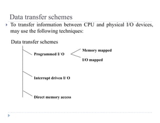
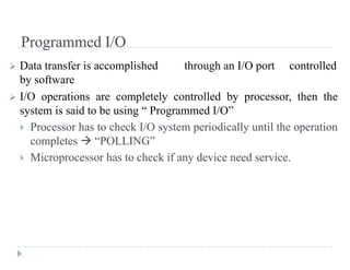
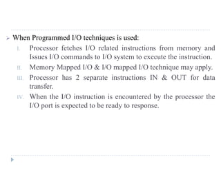
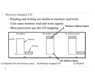
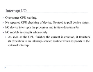
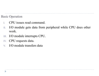
MODULE 3 MCA-203 MICROPROCESSORS AND EMBEDDED SYSTEM ADMN 2014-‘17
Dept. of Computer Science And Applications, SJCET, Palai Page 45
3.1 DATA TRANSFER SCHEMES
• To transfer information between CPU and physical I/O devices, may use the following techniques:
Programmed I/O
 Data transfer is accomplished through an I/O port controlled by software
 The CPU issues a command then waits for I/O operations to be complete.
 Each device given unique identifier
 CPU commands contain identifier (address)
 As the CPU is faster than the I/O module, the CPU has to wait a long time for the I/O module of
concern to be ready for either reception or transmission of data.
 The CPU, while waiting, must repeatedly check the status of the I/O module, and this process is
known as Polling.
Programmed I/O basically works in these ways:
i. CPU requests I/O operation
ii. I/O module performs operation
iii. I/O module sets status bits
iv. CPU checks status bits periodically
v. I/O module does not inform CPU directly
vi. I/O module does not interrupt CPU
vii. CPU may wait or come back later
Fig 1. Flowchart for programmed I/O
CPU issues command that contains
MODULE 3 MCA-203 MICROPROCESSORS AND EMBEDDED SYSTEM ADMN 2014-‘17
Dept. of Computer Science And Applications, SJCET, Palai Page 46
• Control - telling module what to do
• Test - check status
• Read/Write-Module transfers data via buffer from/to device
Advantage
• easy to program and understand
Disadvantages
• slow and inefficient
Interrupt driven I/O
 Overcomes CPU waiting.
 No repeated CPU checking of device, No need to poll device status.
 I/O device interrupts the processor and initiate data transfer
 I/O module interrupts when ready
Basic Operation
I. CPU issues read command.
II. I/O module gets data from peripheral while CPU does other work.
III. I/O module interrupts CPU.
IV. CPU requests data.
V. I/O module transfers data
Fig 2 flow chart for programmed I/O
Advantage
• fast and efficient
Disadvantage
• Difficult to program
Direct Memory Access
 It is a technique of transferring data between memory and I/O devices without CPU intervention.
 DMA controller: dedicated hardware used for controlling the DMA operation.
MODULE 3 MCA-203 MICROPROCESSORS AND EMBEDDED SYSTEM ADMN 2014-‘17
Dept. of Computer Science And Applications, SJCET, Palai Page 47
 DMA channel: system pathway used by a device to transfer information directly to and from
memory.
DMA Operation
• CPU tells DMA controller:-
• Read/Write
• Device address
• Starting address of memory block for data
• Amount of data to be transferred
• CPU carries on with other work
• DMA controller deals with transfer
• DMA controller sends interrupt when finished
Fig 3 flow chart for DMA
DMA Configurations
1. Single Bus, Detached DMA controller
 Each transfer uses bus twice
• I/O to DMA then DMA to memory
• CPU is suspended twice
Fig 4 DMA configuration
2. Single Bus, Integrated DMA controller
• Controller may support >1 device
• Each transfer uses bus once
• DMA to memory
• CPU is suspended once
Fig 5 DMA configuration
MODULE 3 MCA-203 MICROPROCESSORS AND EMBEDDED SYSTEM ADMN 2014-‘17
Dept. of Computer Science And Applications, SJCET, Palai Page 48
3. Separate I/O Bus
• Bus supports all DMA enabled devices
• Each transfer uses bus once
• DMA to memory
• CPU is suspended once
Fig 6 DMA configuration
2.2 DMA CONTROLLER 8257
Features:
 It is a 4-channel DMA.So 4 I/O devices can be interfaced to DMA.
 Have 8bit data line and 16 bit address line.
 Each channel has 16-bit address and 14 bit counter.
 It execute 3 DMA cycles
1. DMA read 2.DMA write 3.DMA verify.
It is operate in two modes.
1. Master Mode
2. Slave Mode
Functional Block diagram
It contains five main Blocks.
1. DMA channels
2. Data bus buffer
3. Read/Write logic
4. Control logic and Mode Set Register
5. Priority resolver
Fig 7 block diagram of 8257
MODULE 3 MCA-203 MICROPROCESSORS AND EMBEDDED SYSTEM ADMN 2014-‘17
Dept. of Computer Science And Applications, SJCET, Palai Page 49
1. DMA channels
 Each of four channels has a pair of two 16-bit registers,
1. DMA address register: store the address of the starting memory location, which will be accessed by
the DMA Channel.
2. Count register: is used to count the number of byte or word transferred by DMA.
The format of count register is,
Fig 8 count register format of 8257
 14-bits B0-B13 is used to count value and a 2-bits is used for indicate the type of DMA transfer
(Read/Write/Verify/illegal transfer).
Pins
DRQ0-DRQ3 (DMA Request)
• The DMA request signals are generated by external peripheral device.
• The DRQ0 has the highest priority while DRQ3 has the lowest one, if the fixed priority mode is
selected.
DACK0-DACK3
• DMA acknowledge output lines.
2 Data Bus Buffer
 It contain 8 bit bi-directional buffer.
 Pins
D0-D7
• Multiplexed data (D0-D7) and address (A8-A15).
i. Slave mode, it transfer data between microprocessor and internal data bus.
ii. Master mode, it act as the higher byte (A8-A15) bits of memory address on data lines.
3 Read/Write Logic
 It controls all internal Read/Write operation.
 Slave mode, it accepts address bits and control signal from microprocessor.
 Master mode, it generate address bits and control signal.
 pins
IOR
• In slave mode, this input signal is used by the CPU to read internal registers of 8257.
• This line acts output in master mode.
IOW
• acts as input in slave mode
• In the master mode, it is a control output
CLK
• input line ,connected with TTL clock generator
RESET
• used to clear mode set registers and status registers
A0-A3
MODULE 3 MCA-203 MICROPROCESSORS AND EMBEDDED SYSTEM ADMN 2014-‘17
Dept. of Computer Science And Applications, SJCET, Palai Page 50
• In slave mode, they act as input which selects one of the registers to be read or written.
• In the master mode, they are the four least significant memory address output lines generated by
8257.
CS
• Chip select line that enables the read/write operations from/to 8257, in slave mode.
• In the master mode, it is automatically disabled to prevent the chip from getting selected (by CPU)
while performing the DMA operation
4 Control logic and Mode Set Register block:
 It contains ,
1. Control logic
2. Mode set register
3. Status Register.
Control Logic
i. Master mode
 It controls the sequence of DMA operation during all DMA cycles.
 It generates address and control signals.
 It increments 16 bit address and decrement 14 bit counter registers.
ii. Slave mode
 it is disabled.
Mode Set Register
 It is a write only registers.
 It is used to set the operating modes.
 This registers is programmed after initialization of DMA channel.
Fig 9 Mode Set register format
AL=1=Auto load mode
AL=0=Rotating mode
TCS=1=Stop after TC (Disable Channel)
TCS=0=Start after TC (Enable Channel)
EW=1=Extended write mode
EW=0=normal mode.
RP=1=Rotating priority
RP=0=Fixed priority.
Status Registers
 It is read only registers, It tell the status of DMA channels.
 These status bits are cleared after a read operation by microprocessor.
 The UP bit is set during update cycle . It is cleared after completion of update cycle.
 TC status bits are set when TC signal is activated for that channel.
EN
3
=1=Enable DMA CH-3
EN
3
=0=Disable DMA CH-3
EN
2
=1=Enable DMA CH-2
EN
2
=0=Disable DMA CH-2
EN
1
=1=Enable DMA CH-1
EN
1
=0=Disable DMA CH-1
EN
0
=1=Enable DMA CH-0
EN
0
=0=Disable DMA CH-0
MODULE 3 MCA-203 MICROPROCESSORS AND EMBEDDED SYSTEM ADMN 2014-‘17
Dept. of Computer Science And Applications, SJCET, Palai Page 51
Fig 10 status register format of 8257
READY
• Used to stretch memory read and write cycles of 8257 by inserting wait states.
• This is used while interfacing slower peripherals..
HRQ
• The hold request output requests the access of the system bus.
HLDA
• It is acknowledgment signal from microprocessor.
AEN (Address enable)
• This output is used to disable the system data bus and the control bus driven by the CPU
ADSTB: (Address Strobe)
• It is a control output line. Used to split data and address line.
TC (Terminal Count)
• It is a status of output line.
• The TC pin is activated when the 14-bit content of the terminal count register of the selected
channel becomes equal to zero.
MARK
• The mark will be activated after each 128 cycles
MEMR
• Memory read output is used to read data from the addressed memory locations during DMA read
cycles.
MEMW
• Memory write output is used to write data to the addressed memory location during DMA write
operation.
A4-A7
• In slave mode, these lines are used as address outputs lines.
• In master mode This is the higher nibble of the lower byte address generated.
5 Priority Resolver
 Resolves the priority of the four DMA channels depending upon whether normal priority or rotating
priority is programmed.
Interfacing 8257 with 8086
• The DMA controller sends a HOLD request to the CPU and waits for the HLDA signal from CPU.
The CPU relinquishes the control of the bus before asserting the HLDA signal.
MODULE 3 MCA-203 MICROPROCESSORS AND EMBEDDED SYSTEM ADMN 2014-‘17
Dept. of Computer Science And Applications, SJCET, Palai Page 52
Fig 11 interfacing 8257 with 8086
• Once the HLDA signal goes high, the DMA controller activates the DACK signal to the requesting
peripheral and gains the control of the system bus.
• The CPU remains in the HOLD status, till the DMA controller is the master of the bus.
2.3 Programmable Interval Timer 8253 (PIT)
Features
1. Three 16-bit independent counters.
2. Three counters are identical pre-settable, and can be programmed for either binary or BCD count.
3. The first timer is usually used as the System Clock. Timer 2 was used for RAM refreshing, and
timer 3 is connected to the PC speaker.
3. Can be programmed in six different modes.
4. Compatible with all Intel and most other microprocessors.
5. Can operate upto 2.6 MHz.
6. Used for controlling real time events such as RT clock, events counter etc
Fig 12 block diagram of 8253
1. Counter
 Each counter is assigned an individual port address.
 Each of the three counters must be programmed separately by writing a control word .
 All counters are down counters.
 Each of the three counter has 3 pins associated
• CLK: input clock frequency
• OUT: can be square wave, or one shot
• GATE: Enable (high) or disable (low) the counter
MODULE 3 MCA-203 MICROPROCESSORS AND EMBEDDED SYSTEM ADMN 2014-‘17
Dept. of Computer Science And Applications, SJCET, Palai Page 53
2. Control word Register
 Allows the programmer to select the counter, mode of operation, binary or BCD count and type of
operation .
 The control register common to all 3 counters and has its own port
Fig 13 control word register format
3. Data Bus Buffer
 Bi-directional, 8-bit buffer is used to interface the 8253 to the system data bus.
 Pins
D0...D7: 8 bit data lines for both read and write operations.
4. Read/Write Logic
 It controls all internal Read/Write operation.
 Pins
• WR: Write enable. When this line is active,
• RD: Read enable. When this line is active
• CS: Chip select signal
• A0, A1: Address lines. Used to determine what register we are accessing.
Operating Modes
Mode 0 Interrupt on terminal count
Mode 1 Programmable one-shot
Mode 2 Rate Generator
Mode 3 Square wave rate generator
Mode 4 Software triggered strobe
Mode 5 Hardware trigger strobe
MODULE 3 MCA-203 MICROPROCESSORS AND EMBEDDED SYSTEM ADMN 2014-‘17
Dept. of Computer Science And Applications, SJCET, Palai Page 54
Mode 0: Interrupt on terminal count
 The output will start off zero. The count is loaded and the timer will start to count down.
 When the count has reached zero the output will be set high, and remain high until the next count
has been reloaded.
Fig 14 Mode 0 operation of 8253
Mode 1: Programmable One-Shot.
 The output will go low following the rising edge of the gate input.
 The counter will count and the output will go high once the counter has reached zero.
Fig 15 Mode 1 operation of 8253
Mode 2: Rate Generator.
 The counter will continually count down, when the count reaches zero, the output will pulse low
and the counter will be reloaded
Fig 16 Mode 2 operation of 8253
Mode 3: Square Wave Generator.
 This mode is similar to Mode 2 except the output remains low for half of the timer period and high
for the other half of the period.
Fig 17 Mode 3 operation of 8253
MODULE 3 MCA-203 MICROPROCESSORS AND EMBEDDED SYSTEM ADMN 2014-‘17
Dept. of Computer Science And Applications, SJCET, Palai Page 55
Mode 4: Software Triggered Pulse.
 The output will remain high until the timer has counted to zero, at which point the output will pulse
low and then go high again.
Fig 18 Mode 4 operation of 8253
Mode 5: Hardware Triggered Pulse.
 The counter will start counting once the gate input goes high, when the counter reaches zero the
output will pulse low and then go high again.
Fig 19 Mode 5 operation of 8253
2.4 PROGRAMMABLE INTERRUPT CONTROLLER 8259
 The Programmable Interrupt Controller (PIC) functions as an overall manager in an Interrupt-
Driven system environment.
 Able to handle a number of interrupts along with their types and priorities at a time.
 Compatible with 8-bit as well as 16-bit processors.
 Deal with up to 64 interrupt inputs.
 Interrupts can be masked.
 Various priority schemes can also program.
BLOCK DIAGRAM
Fig 20 block diagram of 8259
It includes 8 blocks.
 Control logic
MODULE 3 MCA-203 MICROPROCESSORS AND EMBEDDED SYSTEM ADMN 2014-‘17
Dept. of Computer Science And Applications, SJCET, Palai Page 56
 Read/Write logic
 Data bus buffer
 Three registers (IRR,ISR and IMR)
 Priority resolver
 Cascade Buffer
1. Interrupt Request Register (IRR) and In-Service Register (ISR)
• The interrupts at the IR input lines are handled by two registers in cascade, the Interrupt Request
Register (lRR) and the In- Service Register (lSR).
• IRR: is used to indicate all the interrupt levels which are requesting service.
• ISR: is used to store all the interrupt levels which are currently being serviced
Pins
IR0-7: interrupt request input lines, generated by peripherals.
2 Priority Resolver
• This logic block determines the priorities of the bits set in the lRR.
• It determines the priorities as dictated by priority mode set by OCWs.
3 Interrupt Mask Register (IMR)
• This register can be programmed by an OCW to store the bits which mask specific interrupts.
• this allows us to focus on executing certain, more important interrupts before executing the
interrupts specified in this register.
4 Control Logic
• It interacts with microprocessor by sending interrupt request and receiving interrupt
acknowledgement
• Pins
INT: Interrupt line, connected to INTR of microprocessor
INTA: Interrupt ack, received active low from microprocessor
5 Data Bus Buffer
• This bidirectional 8-bit buffer is used to interface the 8259A to the system Data Bus.
• Control words and status information are transferred through the Data Bus Buffer
• Pins
D0-D7:Bi-directional buffered data lines.
6 Read-Write Logic
• Accept output commands from the CPU.
• Contains the Initialization Command Word (ICW) registers and Operation Command Word (OCW)
registers which store the various control formats for device operation.
• pins
WR: Active low write control
RD: Active low read control
A0: Address input line, used to select control register.
CS: Active low chip select
7 The Cascade Buffer/Comparator
• Stores and compares the IDs of all 8259A's used in the system.
• Pins
CAS0-2: are outputs when the 8259A is used as a master and are inputs when the 8259A is used as a slave.
SP/EN: Slave program / enable. In non-buffered mode, it is SP-bar input, used to distinguish master/slave
MODULE 3 MCA-203 MICROPROCESSORS AND EMBEDDED SYSTEM ADMN 2014-‘17
Dept. of Computer Science And Applications, SJCET, Palai Page 57
PIC. In buffered mode, it is output line used to enable buffers.
Command Words
• Two types
1. Initialization Command Word (ICW)
• Used to set up proper conditions
• Before start functioning, 8259 must be initialized by writing two to four command words into their
respective command word registers.
• If there are multiple PICs in the system that are to be cascaded with each other, we must send the
ICW's to both of the PICs.
• ICW 1:is the primary control word used to initialize the PIC
• ICW2:stores the details of interrupt vector addresses.
• ICW3:used to let the PICs know what IRQ lines to use when communicating with each other.
• ICW4:This controls how everything is to operate.
2. Operation Command Word(OCW)
• Used to perform functions such as masking interrupts, setting up status read operations etc.
• There are 3 OCWs
• OCW1 : used to mask the unwanted interrupts
• OCW2 : used to determine the interrupt level
• OCW3 : used to control the mode of 8259A
Operating modes
1. FULLY NESTED
2. AUTOMATIC ROTATION
3. SPECIFIC ROTATION
4. END OF INTERRUPT
5. AUTOMATIC EOI
1. FULLY NESTED
• General purpose mode, All IRs are arranged from highest to lowest.
• IR0 Highest IR7Lowest
2. AUTOMATIC ROTATION MODE
• In this mode, a device after being serviced, receives the lowest priority.
3. SPECIFIC ROTATION MODE
• Similar to automatic rotation mode, except that the user can select any IR for the lowest priority,
thus fixing all other priorities.
4. END OF INTERRUPT (EOI)
• After the completion of an interrupt service, the corresponding ISR bits needs to be reset to update
the information in the ISR. This is called EOI command
5. AUTOMATIC EOI
• In this mode, no command is necessary.
• During the third interrupt acknowledge cycle, the ISR bit is reset.
Interfacing 8259 with 8086
• When an interrupt occurs, the PIC determines the highest priority, activates the processor via its
INTR input, and sends the type number onto the data bus when the processor acknowledges the
interrupt.
MODULE 3 MCA-203 MICROPROCESSORS AND EMBEDDED SYSTEM ADMN 2014-‘17
Dept. of Computer Science And Applications, SJCET, Palai Page 58
Fig 21 interfacing 8259 with 8086
Interrupt Sequence
1. One or more of the IR lines are raised high, setting the corresponding IRR bit(s).
2. The 8259A evaluates these requests, and sends an INT to the CPU, if appropriate.
3. The CPU acknowledges the INT and responds with an INTA pulse.
4. Upon receiving an INTA from the CPU, the highest priority ISR bit is set and the corresponding IRR bit
is reset.
5 The 8086 will send two INTA pulses. During this period 8259 releases an 8 bit pointer on to the data
bus
6. This completes the interrupt cycle. In the AEOI (Automatic End of Interrupt) mode the ISR bit is reset at
the end of the third INTA pulse. Otherwise, the ISR bit remains set until an appropriate EOI (End of
Interrupt Mode) command is issued at the end of the interrupt subroutine.
2.5 8251A PROGRAMMABLE COMMUNICATION INTERFACE
 USART (Universal Synchronous Asynchronous Receiver Transmitter)
 Designed for synchronous /asynchronous serial data communication, packaged in a 28-pin DIP.
 Receives parallel data from the CPU & transmits serial data after conversion.
 Also receives serial data from the outside & transmits parallel data to the CPU after conversion.
Fig 22 block diagram of 8251
Block diagram
Functional Blocks of 8251A
 Data Bus buffer
MODULE 3 MCA-203 MICROPROCESSORS AND EMBEDDED SYSTEM ADMN 2014-‘17
Dept. of Computer Science And Applications, SJCET, Palai Page 59
 Read/Write Control Logic
 Modem Control
 Transmitter
 Receiver
1 Data Bus Buffer
• D0-D7 : 8-bit data bus used to read or write status, command word or data from or to the 8251A
2. Read/Write Control logic
• Includes
a) control logic
b) Status register
c) Data register
d) Control register.
a. Control logic
• Interfaces the chip with MPU,
• Determines the functions of the chip according to the control word in the control register &
monitors the data flow.
b. Status register
• Checks the ready status of the peripheral.
• Status word in the status register provides the information concerning register status and
transmission errors.
c. Data register
• Used as an input and output port when the C/D is low
d. Control Register
• 16-bit register for a control word consist of two independent bytes namely mode word & command
word.
i. Mode word: used for setting the function of the 8251. It controls baud rate, character length, parity
check and number of stop bits
ii. Command word: used for setting the operation of the 8251 ie Enables the data transmission,
reception, error reset and internal reset.
Pins
• RESET: A high on this signal reset 8252A & forces it into the idle mode.
• CLK: Clock input, usually connected to the system clock for communication with the
microprocessor.
• CS – Chip Select: When signal goes low, the 8251A is selected by the MPU for communication.
• C/D – Control/Data: When signal is high, the control or status register is addressed; when it is low,
data buffer is addressed. (Control register & status register are differentiated by WR and RD
signals)
• WR: When signal is low, the MPU either writes in the control register or sends output to the data
buffer.
• RD: When signal goes low, the MPU either reads a status from the status register or accepts data
from data buffer.
MODULE 3 MCA-203 MICROPROCESSORS AND EMBEDDED SYSTEM ADMN 2014-‘17
Dept. of Computer Science And Applications, SJCET, Palai Page 60
3. Modem control
• The modem control unit handles the modem handshake signals to coordinate the communication
between the modem and the 8251.
Pins
DSR - Data Set Ready: when it goes low it means that the Data Set is ready when communicating with a
modem.
DTR - Data Terminal Ready: Indicates that the device is ready to accept data when the 8251 is
communicating with a modem.
CTS - Clear to Send: If its low, the 8251A is enabled to transmit the serial data.
RTS - Request to Send Data: Low signal indicates the modem that the receiver is ready to receive a data
byte from the modem.
4. Transmitter section
• Accepts parallel data from MPU & converts them into serial data.
• Has two registers:
 Buffer register : To hold eight bits
 Output register : To convert eight bits into a stream of serial bits.
 The MPU writes a byte in the buffer register.
 Whenever the output register is empty; the contents of buffer register are transferred to
output register.
Pins
• TxD - Transmitted Data Output : Output signal to transmit the data to peripherals
• TxC - Transmitter Clock Input : Input signal, controls the rate of transmission.
• TxRDY - Transmitter Ready : Output signal, indicates the buffer register is empty and the USART
is ready to accept the next data byte.
• TxE - Transmitter Empty : Output signal to indicate the output register is empty and the USART is
ready to accept the next data byte.
5. Receiver Section
 Accepts serial data on the RxD pin and converts them to parallel data.
 Has two registers :
 Receiver input register
 Buffer register
Pins
• RxRDY - Receiver Ready Output: Output signal, goes high when the USART has a data in the
buffer register & is ready to transfer it to the MPU.
• RxD - Receive Data Input : Bits are received serially on this line & converted into a parallel byte in
the receiver input register.
MODULE 3 MCA-203 MICROPROCESSORS AND EMBEDDED SYSTEM ADMN 2014-‘17
Dept. of Computer Science And Applications, SJCET, Palai Page 61
• RxC - Receiver Clock Input : Clock signal that controls the rate at which bits are received by the 
USART.
2.6 8255-PROGRAMMABLE PERIPHERAL INTERFACE
• Used for interfacing I/O devices with microprocessor.
• Is used to interface to the keyboard and a parallel printer port in PCs (usually as part of an
integrated chipset).
• PPI has 24 pins for I/O.
• can work in 2 modes that are I/O mode and BSR mode
Functional Blocks
• Data Bus Buffer
• Read/Write Control Logic
• Group A and Group B Control
• Port A,B, and C
Fig 23 block diagram of 8255
Data Bus buffer
• It is a 8-bit bidirectional Data bus. Used to interface between 8255 data bus with system bus.
• The direction of data buffer is decided by Read/Control Logic.
Pins
• D0-D7
Read/Write Control Logic
• This is getting the input signals from control bus and Address bus
• Control signal are RD and WR.
• Address signals are A0,A1,and CS.
• CS :8255 operation is enabled (when 0)or disabled(when 1).
• RD and WR are control signal for read and write operations
• A0-A1 used for addressing ports and control register
MODULE 3 MCA-203 MICROPROCESSORS AND EMBEDDED SYSTEM ADMN 2014-‘17
Dept. of Computer Science And Applications, SJCET, Palai Page 62
Group A and Group B control:
• Group A and B get the Control Signal from CPU and send the command to the ports.
• Group A send the control word to port A and Port C (Upper).
• Group B send the control word to port B and Port C (Lower).
• The control word register has two formats. The first format is valid for I/O modes of operation, i.e.
modes 0, mode 1 and mode 2 while the second format is valid for bit set/reset (BSR) mode of
operation
PORT A:
 This is a 8-bit buffered I/O latch.
PORT B:
• This is a 8-bit buffer I/O latch.
PORT C:
• This is a 8-bit buffer Input and an Output latch.
• It is spitted into two parts upper and lower.
Operating modes:
• I/O Mode Control Word Register Format – The I/O modes can be programmed using control word
register by putting D7 at logic 1. Format is shown below:
Fig 24 I/O mode control word format
MODULE 3 MCA-203 MICROPROCESSORS AND EMBEDDED SYSTEM ADMN 2014-‘17
Dept. of Computer Science And Applications, SJCET, Palai Page 63
1. MODE 0(Basic input / Output):
• Ports A, B, and C can be individually programmed as input or output ports
• Outputs are latched, Inputs are buffered not latched.
• There is no handshake signals
2. MODE 1 :( Input/output with Handshakes)
• Input or output is transferred by hand shaking Signals.
• Input and Output data are latched.
• Ports A and B are programmed as input or output ports and Port C is used for handshaking
3. MODE 2 (bi-directional I/O data transfer)
• This mode allows bidirectional data transfer over a single 8-bit data bus using handshake signals.
• This feature is possible only Group A
• Port A is working as 8-bit bidirectional.
• PC3-PC7 is used for handshaking purpose

Module 3 special purpose programmable devices and their interfacing

  • 1.
    MODULE 3 MCA-203MICROPROCESSORS AND EMBEDDED SYSTEM ADMN 2014-‘17 Dept. of Computer Science And Applications, SJCET, Palai Page 45 3.1 DATA TRANSFER SCHEMES • To transfer information between CPU and physical I/O devices, may use the following techniques: Programmed I/O  Data transfer is accomplished through an I/O port controlled by software  The CPU issues a command then waits for I/O operations to be complete.  Each device given unique identifier  CPU commands contain identifier (address)  As the CPU is faster than the I/O module, the CPU has to wait a long time for the I/O module of concern to be ready for either reception or transmission of data.  The CPU, while waiting, must repeatedly check the status of the I/O module, and this process is known as Polling. Programmed I/O basically works in these ways: i. CPU requests I/O operation ii. I/O module performs operation iii. I/O module sets status bits iv. CPU checks status bits periodically v. I/O module does not inform CPU directly vi. I/O module does not interrupt CPU vii. CPU may wait or come back later Fig 1. Flowchart for programmed I/O CPU issues command that contains
  • 2.
    MODULE 3 MCA-203MICROPROCESSORS AND EMBEDDED SYSTEM ADMN 2014-‘17 Dept. of Computer Science And Applications, SJCET, Palai Page 46 • Control - telling module what to do • Test - check status • Read/Write-Module transfers data via buffer from/to device Advantage • easy to program and understand Disadvantages • slow and inefficient Interrupt driven I/O  Overcomes CPU waiting.  No repeated CPU checking of device, No need to poll device status.  I/O device interrupts the processor and initiate data transfer  I/O module interrupts when ready Basic Operation I. CPU issues read command. II. I/O module gets data from peripheral while CPU does other work. III. I/O module interrupts CPU. IV. CPU requests data. V. I/O module transfers data Fig 2 flow chart for programmed I/O Advantage • fast and efficient Disadvantage • Difficult to program Direct Memory Access  It is a technique of transferring data between memory and I/O devices without CPU intervention.  DMA controller: dedicated hardware used for controlling the DMA operation.
  • 3.
    MODULE 3 MCA-203MICROPROCESSORS AND EMBEDDED SYSTEM ADMN 2014-‘17 Dept. of Computer Science And Applications, SJCET, Palai Page 47  DMA channel: system pathway used by a device to transfer information directly to and from memory. DMA Operation • CPU tells DMA controller:- • Read/Write • Device address • Starting address of memory block for data • Amount of data to be transferred • CPU carries on with other work • DMA controller deals with transfer • DMA controller sends interrupt when finished Fig 3 flow chart for DMA DMA Configurations 1. Single Bus, Detached DMA controller  Each transfer uses bus twice • I/O to DMA then DMA to memory • CPU is suspended twice Fig 4 DMA configuration 2. Single Bus, Integrated DMA controller • Controller may support >1 device • Each transfer uses bus once • DMA to memory • CPU is suspended once Fig 5 DMA configuration
  • 4.
    MODULE 3 MCA-203MICROPROCESSORS AND EMBEDDED SYSTEM ADMN 2014-‘17 Dept. of Computer Science And Applications, SJCET, Palai Page 48 3. Separate I/O Bus • Bus supports all DMA enabled devices • Each transfer uses bus once • DMA to memory • CPU is suspended once Fig 6 DMA configuration 2.2 DMA CONTROLLER 8257 Features:  It is a 4-channel DMA.So 4 I/O devices can be interfaced to DMA.  Have 8bit data line and 16 bit address line.  Each channel has 16-bit address and 14 bit counter.  It execute 3 DMA cycles 1. DMA read 2.DMA write 3.DMA verify. It is operate in two modes. 1. Master Mode 2. Slave Mode Functional Block diagram It contains five main Blocks. 1. DMA channels 2. Data bus buffer 3. Read/Write logic 4. Control logic and Mode Set Register 5. Priority resolver Fig 7 block diagram of 8257
  • 5.
    MODULE 3 MCA-203MICROPROCESSORS AND EMBEDDED SYSTEM ADMN 2014-‘17 Dept. of Computer Science And Applications, SJCET, Palai Page 49 1. DMA channels  Each of four channels has a pair of two 16-bit registers, 1. DMA address register: store the address of the starting memory location, which will be accessed by the DMA Channel. 2. Count register: is used to count the number of byte or word transferred by DMA. The format of count register is, Fig 8 count register format of 8257  14-bits B0-B13 is used to count value and a 2-bits is used for indicate the type of DMA transfer (Read/Write/Verify/illegal transfer). Pins DRQ0-DRQ3 (DMA Request) • The DMA request signals are generated by external peripheral device. • The DRQ0 has the highest priority while DRQ3 has the lowest one, if the fixed priority mode is selected. DACK0-DACK3 • DMA acknowledge output lines. 2 Data Bus Buffer  It contain 8 bit bi-directional buffer.  Pins D0-D7 • Multiplexed data (D0-D7) and address (A8-A15). i. Slave mode, it transfer data between microprocessor and internal data bus. ii. Master mode, it act as the higher byte (A8-A15) bits of memory address on data lines. 3 Read/Write Logic  It controls all internal Read/Write operation.  Slave mode, it accepts address bits and control signal from microprocessor.  Master mode, it generate address bits and control signal.  pins IOR • In slave mode, this input signal is used by the CPU to read internal registers of 8257. • This line acts output in master mode. IOW • acts as input in slave mode • In the master mode, it is a control output CLK • input line ,connected with TTL clock generator RESET • used to clear mode set registers and status registers A0-A3
  • 6.
    MODULE 3 MCA-203MICROPROCESSORS AND EMBEDDED SYSTEM ADMN 2014-‘17 Dept. of Computer Science And Applications, SJCET, Palai Page 50 • In slave mode, they act as input which selects one of the registers to be read or written. • In the master mode, they are the four least significant memory address output lines generated by 8257. CS • Chip select line that enables the read/write operations from/to 8257, in slave mode. • In the master mode, it is automatically disabled to prevent the chip from getting selected (by CPU) while performing the DMA operation 4 Control logic and Mode Set Register block:  It contains , 1. Control logic 2. Mode set register 3. Status Register. Control Logic i. Master mode  It controls the sequence of DMA operation during all DMA cycles.  It generates address and control signals.  It increments 16 bit address and decrement 14 bit counter registers. ii. Slave mode  it is disabled. Mode Set Register  It is a write only registers.  It is used to set the operating modes.  This registers is programmed after initialization of DMA channel. Fig 9 Mode Set register format AL=1=Auto load mode AL=0=Rotating mode TCS=1=Stop after TC (Disable Channel) TCS=0=Start after TC (Enable Channel) EW=1=Extended write mode EW=0=normal mode. RP=1=Rotating priority RP=0=Fixed priority. Status Registers  It is read only registers, It tell the status of DMA channels.  These status bits are cleared after a read operation by microprocessor.  The UP bit is set during update cycle . It is cleared after completion of update cycle.  TC status bits are set when TC signal is activated for that channel. EN 3 =1=Enable DMA CH-3 EN 3 =0=Disable DMA CH-3 EN 2 =1=Enable DMA CH-2 EN 2 =0=Disable DMA CH-2 EN 1 =1=Enable DMA CH-1 EN 1 =0=Disable DMA CH-1 EN 0 =1=Enable DMA CH-0 EN 0 =0=Disable DMA CH-0
  • 7.
    MODULE 3 MCA-203MICROPROCESSORS AND EMBEDDED SYSTEM ADMN 2014-‘17 Dept. of Computer Science And Applications, SJCET, Palai Page 51 Fig 10 status register format of 8257 READY • Used to stretch memory read and write cycles of 8257 by inserting wait states. • This is used while interfacing slower peripherals.. HRQ • The hold request output requests the access of the system bus. HLDA • It is acknowledgment signal from microprocessor. AEN (Address enable) • This output is used to disable the system data bus and the control bus driven by the CPU ADSTB: (Address Strobe) • It is a control output line. Used to split data and address line. TC (Terminal Count) • It is a status of output line. • The TC pin is activated when the 14-bit content of the terminal count register of the selected channel becomes equal to zero. MARK • The mark will be activated after each 128 cycles MEMR • Memory read output is used to read data from the addressed memory locations during DMA read cycles. MEMW • Memory write output is used to write data to the addressed memory location during DMA write operation. A4-A7 • In slave mode, these lines are used as address outputs lines. • In master mode This is the higher nibble of the lower byte address generated. 5 Priority Resolver  Resolves the priority of the four DMA channels depending upon whether normal priority or rotating priority is programmed. Interfacing 8257 with 8086 • The DMA controller sends a HOLD request to the CPU and waits for the HLDA signal from CPU. The CPU relinquishes the control of the bus before asserting the HLDA signal.
  • 8.
    MODULE 3 MCA-203MICROPROCESSORS AND EMBEDDED SYSTEM ADMN 2014-‘17 Dept. of Computer Science And Applications, SJCET, Palai Page 52 Fig 11 interfacing 8257 with 8086 • Once the HLDA signal goes high, the DMA controller activates the DACK signal to the requesting peripheral and gains the control of the system bus. • The CPU remains in the HOLD status, till the DMA controller is the master of the bus. 2.3 Programmable Interval Timer 8253 (PIT) Features 1. Three 16-bit independent counters. 2. Three counters are identical pre-settable, and can be programmed for either binary or BCD count. 3. The first timer is usually used as the System Clock. Timer 2 was used for RAM refreshing, and timer 3 is connected to the PC speaker. 3. Can be programmed in six different modes. 4. Compatible with all Intel and most other microprocessors. 5. Can operate upto 2.6 MHz. 6. Used for controlling real time events such as RT clock, events counter etc Fig 12 block diagram of 8253 1. Counter  Each counter is assigned an individual port address.  Each of the three counters must be programmed separately by writing a control word .  All counters are down counters.  Each of the three counter has 3 pins associated • CLK: input clock frequency • OUT: can be square wave, or one shot • GATE: Enable (high) or disable (low) the counter
  • 9.
    MODULE 3 MCA-203MICROPROCESSORS AND EMBEDDED SYSTEM ADMN 2014-‘17 Dept. of Computer Science And Applications, SJCET, Palai Page 53 2. Control word Register  Allows the programmer to select the counter, mode of operation, binary or BCD count and type of operation .  The control register common to all 3 counters and has its own port Fig 13 control word register format 3. Data Bus Buffer  Bi-directional, 8-bit buffer is used to interface the 8253 to the system data bus.  Pins D0...D7: 8 bit data lines for both read and write operations. 4. Read/Write Logic  It controls all internal Read/Write operation.  Pins • WR: Write enable. When this line is active, • RD: Read enable. When this line is active • CS: Chip select signal • A0, A1: Address lines. Used to determine what register we are accessing. Operating Modes Mode 0 Interrupt on terminal count Mode 1 Programmable one-shot Mode 2 Rate Generator Mode 3 Square wave rate generator Mode 4 Software triggered strobe Mode 5 Hardware trigger strobe
  • 10.
    MODULE 3 MCA-203MICROPROCESSORS AND EMBEDDED SYSTEM ADMN 2014-‘17 Dept. of Computer Science And Applications, SJCET, Palai Page 54 Mode 0: Interrupt on terminal count  The output will start off zero. The count is loaded and the timer will start to count down.  When the count has reached zero the output will be set high, and remain high until the next count has been reloaded. Fig 14 Mode 0 operation of 8253 Mode 1: Programmable One-Shot.  The output will go low following the rising edge of the gate input.  The counter will count and the output will go high once the counter has reached zero. Fig 15 Mode 1 operation of 8253 Mode 2: Rate Generator.  The counter will continually count down, when the count reaches zero, the output will pulse low and the counter will be reloaded Fig 16 Mode 2 operation of 8253 Mode 3: Square Wave Generator.  This mode is similar to Mode 2 except the output remains low for half of the timer period and high for the other half of the period. Fig 17 Mode 3 operation of 8253
  • 11.
    MODULE 3 MCA-203MICROPROCESSORS AND EMBEDDED SYSTEM ADMN 2014-‘17 Dept. of Computer Science And Applications, SJCET, Palai Page 55 Mode 4: Software Triggered Pulse.  The output will remain high until the timer has counted to zero, at which point the output will pulse low and then go high again. Fig 18 Mode 4 operation of 8253 Mode 5: Hardware Triggered Pulse.  The counter will start counting once the gate input goes high, when the counter reaches zero the output will pulse low and then go high again. Fig 19 Mode 5 operation of 8253 2.4 PROGRAMMABLE INTERRUPT CONTROLLER 8259  The Programmable Interrupt Controller (PIC) functions as an overall manager in an Interrupt- Driven system environment.  Able to handle a number of interrupts along with their types and priorities at a time.  Compatible with 8-bit as well as 16-bit processors.  Deal with up to 64 interrupt inputs.  Interrupts can be masked.  Various priority schemes can also program. BLOCK DIAGRAM Fig 20 block diagram of 8259 It includes 8 blocks.  Control logic
  • 12.
    MODULE 3 MCA-203MICROPROCESSORS AND EMBEDDED SYSTEM ADMN 2014-‘17 Dept. of Computer Science And Applications, SJCET, Palai Page 56  Read/Write logic  Data bus buffer  Three registers (IRR,ISR and IMR)  Priority resolver  Cascade Buffer 1. Interrupt Request Register (IRR) and In-Service Register (ISR) • The interrupts at the IR input lines are handled by two registers in cascade, the Interrupt Request Register (lRR) and the In- Service Register (lSR). • IRR: is used to indicate all the interrupt levels which are requesting service. • ISR: is used to store all the interrupt levels which are currently being serviced Pins IR0-7: interrupt request input lines, generated by peripherals. 2 Priority Resolver • This logic block determines the priorities of the bits set in the lRR. • It determines the priorities as dictated by priority mode set by OCWs. 3 Interrupt Mask Register (IMR) • This register can be programmed by an OCW to store the bits which mask specific interrupts. • this allows us to focus on executing certain, more important interrupts before executing the interrupts specified in this register. 4 Control Logic • It interacts with microprocessor by sending interrupt request and receiving interrupt acknowledgement • Pins INT: Interrupt line, connected to INTR of microprocessor INTA: Interrupt ack, received active low from microprocessor 5 Data Bus Buffer • This bidirectional 8-bit buffer is used to interface the 8259A to the system Data Bus. • Control words and status information are transferred through the Data Bus Buffer • Pins D0-D7:Bi-directional buffered data lines. 6 Read-Write Logic • Accept output commands from the CPU. • Contains the Initialization Command Word (ICW) registers and Operation Command Word (OCW) registers which store the various control formats for device operation. • pins WR: Active low write control RD: Active low read control A0: Address input line, used to select control register. CS: Active low chip select 7 The Cascade Buffer/Comparator • Stores and compares the IDs of all 8259A's used in the system. • Pins CAS0-2: are outputs when the 8259A is used as a master and are inputs when the 8259A is used as a slave. SP/EN: Slave program / enable. In non-buffered mode, it is SP-bar input, used to distinguish master/slave
  • 13.
    MODULE 3 MCA-203MICROPROCESSORS AND EMBEDDED SYSTEM ADMN 2014-‘17 Dept. of Computer Science And Applications, SJCET, Palai Page 57 PIC. In buffered mode, it is output line used to enable buffers. Command Words • Two types 1. Initialization Command Word (ICW) • Used to set up proper conditions • Before start functioning, 8259 must be initialized by writing two to four command words into their respective command word registers. • If there are multiple PICs in the system that are to be cascaded with each other, we must send the ICW's to both of the PICs. • ICW 1:is the primary control word used to initialize the PIC • ICW2:stores the details of interrupt vector addresses. • ICW3:used to let the PICs know what IRQ lines to use when communicating with each other. • ICW4:This controls how everything is to operate. 2. Operation Command Word(OCW) • Used to perform functions such as masking interrupts, setting up status read operations etc. • There are 3 OCWs • OCW1 : used to mask the unwanted interrupts • OCW2 : used to determine the interrupt level • OCW3 : used to control the mode of 8259A Operating modes 1. FULLY NESTED 2. AUTOMATIC ROTATION 3. SPECIFIC ROTATION 4. END OF INTERRUPT 5. AUTOMATIC EOI 1. FULLY NESTED • General purpose mode, All IRs are arranged from highest to lowest. • IR0 Highest IR7Lowest 2. AUTOMATIC ROTATION MODE • In this mode, a device after being serviced, receives the lowest priority. 3. SPECIFIC ROTATION MODE • Similar to automatic rotation mode, except that the user can select any IR for the lowest priority, thus fixing all other priorities. 4. END OF INTERRUPT (EOI) • After the completion of an interrupt service, the corresponding ISR bits needs to be reset to update the information in the ISR. This is called EOI command 5. AUTOMATIC EOI • In this mode, no command is necessary. • During the third interrupt acknowledge cycle, the ISR bit is reset. Interfacing 8259 with 8086 • When an interrupt occurs, the PIC determines the highest priority, activates the processor via its INTR input, and sends the type number onto the data bus when the processor acknowledges the interrupt.
  • 14.
    MODULE 3 MCA-203MICROPROCESSORS AND EMBEDDED SYSTEM ADMN 2014-‘17 Dept. of Computer Science And Applications, SJCET, Palai Page 58 Fig 21 interfacing 8259 with 8086 Interrupt Sequence 1. One or more of the IR lines are raised high, setting the corresponding IRR bit(s). 2. The 8259A evaluates these requests, and sends an INT to the CPU, if appropriate. 3. The CPU acknowledges the INT and responds with an INTA pulse. 4. Upon receiving an INTA from the CPU, the highest priority ISR bit is set and the corresponding IRR bit is reset. 5 The 8086 will send two INTA pulses. During this period 8259 releases an 8 bit pointer on to the data bus 6. This completes the interrupt cycle. In the AEOI (Automatic End of Interrupt) mode the ISR bit is reset at the end of the third INTA pulse. Otherwise, the ISR bit remains set until an appropriate EOI (End of Interrupt Mode) command is issued at the end of the interrupt subroutine. 2.5 8251A PROGRAMMABLE COMMUNICATION INTERFACE  USART (Universal Synchronous Asynchronous Receiver Transmitter)  Designed for synchronous /asynchronous serial data communication, packaged in a 28-pin DIP.  Receives parallel data from the CPU & transmits serial data after conversion.  Also receives serial data from the outside & transmits parallel data to the CPU after conversion. Fig 22 block diagram of 8251 Block diagram Functional Blocks of 8251A  Data Bus buffer
  • 15.
    MODULE 3 MCA-203MICROPROCESSORS AND EMBEDDED SYSTEM ADMN 2014-‘17 Dept. of Computer Science And Applications, SJCET, Palai Page 59  Read/Write Control Logic  Modem Control  Transmitter  Receiver 1 Data Bus Buffer • D0-D7 : 8-bit data bus used to read or write status, command word or data from or to the 8251A 2. Read/Write Control logic • Includes a) control logic b) Status register c) Data register d) Control register. a. Control logic • Interfaces the chip with MPU, • Determines the functions of the chip according to the control word in the control register & monitors the data flow. b. Status register • Checks the ready status of the peripheral. • Status word in the status register provides the information concerning register status and transmission errors. c. Data register • Used as an input and output port when the C/D is low d. Control Register • 16-bit register for a control word consist of two independent bytes namely mode word & command word. i. Mode word: used for setting the function of the 8251. It controls baud rate, character length, parity check and number of stop bits ii. Command word: used for setting the operation of the 8251 ie Enables the data transmission, reception, error reset and internal reset. Pins • RESET: A high on this signal reset 8252A & forces it into the idle mode. • CLK: Clock input, usually connected to the system clock for communication with the microprocessor. • CS – Chip Select: When signal goes low, the 8251A is selected by the MPU for communication. • C/D – Control/Data: When signal is high, the control or status register is addressed; when it is low, data buffer is addressed. (Control register & status register are differentiated by WR and RD signals) • WR: When signal is low, the MPU either writes in the control register or sends output to the data buffer. • RD: When signal goes low, the MPU either reads a status from the status register or accepts data from data buffer.
  • 16.
    MODULE 3 MCA-203MICROPROCESSORS AND EMBEDDED SYSTEM ADMN 2014-‘17 Dept. of Computer Science And Applications, SJCET, Palai Page 60 3. Modem control • The modem control unit handles the modem handshake signals to coordinate the communication between the modem and the 8251. Pins DSR - Data Set Ready: when it goes low it means that the Data Set is ready when communicating with a modem. DTR - Data Terminal Ready: Indicates that the device is ready to accept data when the 8251 is communicating with a modem. CTS - Clear to Send: If its low, the 8251A is enabled to transmit the serial data. RTS - Request to Send Data: Low signal indicates the modem that the receiver is ready to receive a data byte from the modem. 4. Transmitter section • Accepts parallel data from MPU & converts them into serial data. • Has two registers:  Buffer register : To hold eight bits  Output register : To convert eight bits into a stream of serial bits.  The MPU writes a byte in the buffer register.  Whenever the output register is empty; the contents of buffer register are transferred to output register. Pins • TxD - Transmitted Data Output : Output signal to transmit the data to peripherals • TxC - Transmitter Clock Input : Input signal, controls the rate of transmission. • TxRDY - Transmitter Ready : Output signal, indicates the buffer register is empty and the USART is ready to accept the next data byte. • TxE - Transmitter Empty : Output signal to indicate the output register is empty and the USART is ready to accept the next data byte. 5. Receiver Section  Accepts serial data on the RxD pin and converts them to parallel data.  Has two registers :  Receiver input register  Buffer register Pins • RxRDY - Receiver Ready Output: Output signal, goes high when the USART has a data in the buffer register & is ready to transfer it to the MPU. • RxD - Receive Data Input : Bits are received serially on this line & converted into a parallel byte in the receiver input register.
  • 17.
    MODULE 3 MCA-203MICROPROCESSORS AND EMBEDDED SYSTEM ADMN 2014-‘17 Dept. of Computer Science And Applications, SJCET, Palai Page 61 • RxC - Receiver Clock Input : Clock signal that controls the rate at which bits are received by the USART. 2.6 8255-PROGRAMMABLE PERIPHERAL INTERFACE • Used for interfacing I/O devices with microprocessor. • Is used to interface to the keyboard and a parallel printer port in PCs (usually as part of an integrated chipset). • PPI has 24 pins for I/O. • can work in 2 modes that are I/O mode and BSR mode Functional Blocks • Data Bus Buffer • Read/Write Control Logic • Group A and Group B Control • Port A,B, and C Fig 23 block diagram of 8255 Data Bus buffer • It is a 8-bit bidirectional Data bus. Used to interface between 8255 data bus with system bus. • The direction of data buffer is decided by Read/Control Logic. Pins • D0-D7 Read/Write Control Logic • This is getting the input signals from control bus and Address bus • Control signal are RD and WR. • Address signals are A0,A1,and CS. • CS :8255 operation is enabled (when 0)or disabled(when 1). • RD and WR are control signal for read and write operations • A0-A1 used for addressing ports and control register
  • 18.
    MODULE 3 MCA-203MICROPROCESSORS AND EMBEDDED SYSTEM ADMN 2014-‘17 Dept. of Computer Science And Applications, SJCET, Palai Page 62 Group A and Group B control: • Group A and B get the Control Signal from CPU and send the command to the ports. • Group A send the control word to port A and Port C (Upper). • Group B send the control word to port B and Port C (Lower). • The control word register has two formats. The first format is valid for I/O modes of operation, i.e. modes 0, mode 1 and mode 2 while the second format is valid for bit set/reset (BSR) mode of operation PORT A:  This is a 8-bit buffered I/O latch. PORT B: • This is a 8-bit buffer I/O latch. PORT C: • This is a 8-bit buffer Input and an Output latch. • It is spitted into two parts upper and lower. Operating modes: • I/O Mode Control Word Register Format – The I/O modes can be programmed using control word register by putting D7 at logic 1. Format is shown below: Fig 24 I/O mode control word format
  • 19.
    MODULE 3 MCA-203MICROPROCESSORS AND EMBEDDED SYSTEM ADMN 2014-‘17 Dept. of Computer Science And Applications, SJCET, Palai Page 63 1. MODE 0(Basic input / Output): • Ports A, B, and C can be individually programmed as input or output ports • Outputs are latched, Inputs are buffered not latched. • There is no handshake signals 2. MODE 1 :( Input/output with Handshakes) • Input or output is transferred by hand shaking Signals. • Input and Output data are latched. • Ports A and B are programmed as input or output ports and Port C is used for handshaking 3. MODE 2 (bi-directional I/O data transfer) • This mode allows bidirectional data transfer over a single 8-bit data bus using handshake signals. • This feature is possible only Group A • Port A is working as 8-bit bidirectional. • PC3-PC7 is used for handshaking purpose