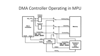
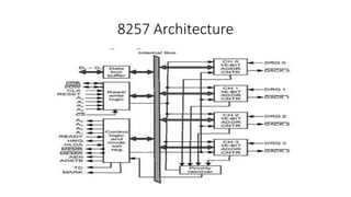
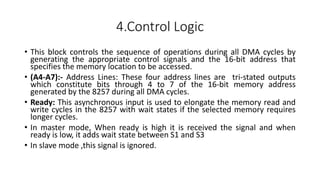
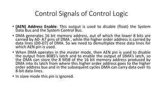
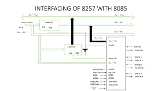
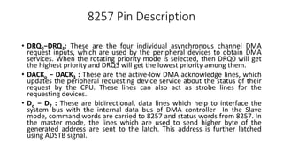
SlideShare a Scribd company logo
8257
DMA Controller
What is DMA
• A direct memory access (DMA) is an operation in which data is copied
(transported) from one resource to another resource in a computer
system without the involvement of the CPU.
• The task of a DMA-controller (DMAC) is to execute the copy operation
of data from one resource location to another. The copy of data can
be performed from:
- I/O-device to memory
- memory to I/O-device
- memory to memory
- I/O-device to I/O-device
Contd.
• A DMAC is an independent (from CPU) resource of a computer system
added for the concurrent execution of DMA-operations.
• The DMAC replaces the CPU for the transfer task of data from the I/O-
device to the main memory (or vice versa) which otherwise would
have been executed by the CPU using the programmed input output
(PIO) mode.
• The CPU initiates the transfer, does other operations while the
transfer is in progress, and receives an interrupt from the DMA
controller when the operation is done.
DMA Initialization
• DMA controllers require initialization by software. Typical setup
parameters include the
• base address of the source area,
• base address of the destination area,
• length of the block, and
• whether the DMA controller should generate a processor interrupt once the
block transfer is complete.
The 8257 offers three different modes of
operation:
• (1) DMA read, which causes data to be transferred from memory to
peripheral:
• (2) DMA write, which causes data to be transferred from peripheral to
memory.
• (3) DMA verify, which does not actually involve the transfer of data.
• When an 8257 channel is in the DMA verify mode, it will respond the same as
described for transfer operations, except that no memory or I/O read/write control
signals will be generated, thus preventing the transfer of data.
• The 8257. however, will gain control of the system bus and will acknowledge the
peripheral's DMA request for each DMA cycle.
• The peripheral can use these acknowledge signals to enable an internal access of
each byte of data block in order to execute some verification procedure, such as the
accumulation of CRC (Cyclic Redundancy Code) checkword.
DMA Controller Operating in MPU
DMA Idle Cycle
• When the system is turned on, the switches are in the A position, so
the buses are connected from the microprocessor to the system
memory and peripherals. Microprocessor then executes the program
until it needs to read a block of data from the disk.
• To read a block of data from the disk microprocessor sends a series of
commands to the disk controller telling it to search and read the
desired block of data from the disk into the disk buffer.
• When the disk controller is ready with the first byte of data in its
buffer, it sends DMA request DRQ signal to the DMA controller.
Execution of a DMA-operation
• Initially, when any device has to send data between the device and
the memory, the device has to send DMA request (DRQ) to DMA
controller.
• The DMA controller sends Hold request (HRQ) to the CPU on HOLD
line and waits for the CPU to assert the HLDA.
• Then the microprocessor tri-states all the data bus, address bus, and
control bus. The CPU leaves the control over bus and acknowledges
the HOLD request through HLDA signal.
• Now the CPU is in HOLD state and the DMA controller has to manage
the operations over buses between the CPU, memory, and I/O
devices.
DMA Active Cycle
• When DMA controller gets control of the buses, it sends the memory
address where the first byte of data from the disk is to be written.
• It also sends DMA acknowledge, DACK signal to the disk controller device
telling it to get ready for data transfer .
• Finally ( in case of DMA write operation ), it asserts both the IOR and
MEMW signals on the control bus . Asserting the IOR signals enables the
disk controller to output the data from the disk on the data bus and
MEMW signal enables the addressed memory to accept data form the data
bus.
• In this technique data is transferred directly from the disk controller to the
memory location without passing through the CPU or the DMA controller.
DMA Controller 8257
• 8257 is a programmable, 4 channel, DMA controller. Each channel can be
programmed independently to transfer up to 64kb of data by DMA.
Therefore we can interface 4 I/O devices with 8257.
• Each channel includes a 16-bit DMA address register and a 14-bit counter.
• DMA address register gives the address of the memory location and
counter specifies the number of DMA cycles to be performed.
• As counter is 14-bit, each channel can transfer 214 (16 kbytes) without
intervention of microprocessor.
• It maintains the DMA cycle count for each channel and activates a control
signal TC (Terminal count) to indicate the peripheral that the programmed
number of DMA cycles are complete.
Contd.
• It provides another control signal MARK to indicate peripheral that the
current DMA cycle is the 128thcycle since the previous MARK output.
• It has priority logic that resolves the peripherals requests. The priority logic
can be programmed to work in two modes, either in fixed mode or rotating
priority mode.
• It allows data transfer in two modes : burst mode and cycle steal (single
byte transfer) mode.
• It can execute three DMA cycles : DMA read, DMA write and DMA verify.
• It operates in two modes : slave and master , where in master mode it
gains control over the system buses while in slave mode buses are under
control of processor
8257 Architecture
The functional block diagram consists of
1. DMA channels
2. Data bus buffer
3. Read/Write logic
4. Control logic
5. Mode set Register
6. Status Register
1. DMA Channels
 The 8257 provides four separate DMA channels (labeled CH-0 to CH-3).
 Each channel includes two sixteen-bit registers:
(1) DMA address register, and
(2) Terminal count register
 Both registers must be initialized before channel is enabled.
 The DMA address register is loaded with the address of the first memory
location to be accessed.
 The value loaded into the low-order 14-bits of the terminal count register
specifies the number of DMA cycles minus one before the Terminal Count (TC)
output is activated.
 In general, if the number of desired DMA cycles, load the value N-1 into the
low-order 14-bits of the terminal count register.
DMA Channels
• The most significant two bits of the terminal count register specify
the type of DMA operation for that channel.
• Each channel accepts DMA Request (DRQn) input and provides DMA
Acknowledge (DACKn) output.
• (DRQ0-DRQ3) : DMA Request: These are individual asynchronous
channel request inputs used by the peripherals to obtain DMA cycle.
• (DACK0- DACK3) :- DMA Acknowledge: An active low level on the
acknowledge output informs the peripheral connected to that
channel that it has been selected for DMA cycle.
Format of Terminal Count Register
• The most significant two bits of the terminal count register specify
the type of DMA operation for that channel.
2. Data Bus Buffer
• This three-state, bi-directional, eight bit buffer interfaces the 8257 to the system
data bus.
(D0-D7) :-
• Data Bus Lines: These are 8-bit bi-directional three-state lines.
• When the 8257 is being programmed by the CPU. Eight bits of data for DMA
address register, terminal count register or the Mode Set register are received on
the data bus.
• When the CPU reads DMA address register, terminal count register or the Status
register, the data is sent to the CPU over the data bus.
• When 8257 is operating as Master, during a DMA cycle, it gains control over the
system buses. In this mode, the 8257 sends out the 8 MSBs of the DMA address
register of the channel being serviced on the D0-D7 pins at the starting of each
DMA cycle to the 8212 latch. After this, the bus is released to handle the
memory data transfer during the remaining DMA cycle.
3. Read/Write Logic
• When the CPU is programming or reading one of the 8257’s registers
(i.e., when the 8257 is "slave" device on the system bus), the
Read/Write Logic accepts the I/O Read or I/O Write signal, decodes
the least significant four address bits, (A0-A3), and either writes the
contents of the data bus into the addressed register (if I/OW is true)
or places the contents of the addressed register onto the data bus (if
I/OR is true).
• During DMA cycles (i.e., when the 8257 is the bus "master"), the
Read/Write Logic generates the I/O read and memory write (DMA
write cycle) or I/O Write and memory read (DMA read cycle) signals
which control the data link with the peripheral that has been granted
the DMA cycle.
Signals of Read/Write Logic
• I/O Read: An active-low, bi-directional three-state line. In the "slave" mode, it is
an input which allows the 8-bit status register or the upper/lower byte of 16-bit
DMA address register or terminal count register to be read.
• In the "master" mode, I/O Read is control output which is used to access data
from peripheral during the DMA write cycle( reading data from I/O and write into
memory).
• I/O Write: An active-low, bi-directional three-state line. In the "slave" mode, it is
an input which allows the contents of the data bus to be loaded into the 8-bit
mode set register or the upper/lower byte of 16-bit DMA address register or
terminal count register.
• In the "master" mode, I/OW is control output which allows data to be output to
peripheral during DMA read cycle (reading from memory and write into I/O).
Signals of Read/Write Logic
• Clock Input: Generally from an Clock Generator device) or Intel 8085A
CLK output.
• Reset: An asynchronous input from 8085 which disables all DMA
channels by clearing the mode register and tri-stated all control lines.
• (A0-A3) :- Address lines:- These least significant four address lines are
bi-directional.
• In the "slave" mode they are inputs which select one of the registers to be
read or programmed.
• In the "master" mode, they are outputs which constitute the least significant
four bits of the 16-bit memory address generated by the 8257.
Signals of Read/Write Logic
• Chip Select:
• It is active low, Chip select input line.
• In the slave mode, it is used to select the chip.
• In the master mode, it is ignored.
4.Control Logic
• This block controls the sequence of operations during all DMA cycles by
generating the appropriate control signals and the 16-bit address that
specifies the memory location to be accessed.
• (A4-A7):- Address Lines: These four address lines are tri-stated outputs
which constitute bits through 4 to 7 of the 16-bit memory address
generated by the 8257 during all DMA cycles.
• Ready: This asynchronous input is used to elongate the memory read and
write cycles in the 8257 with wait states if the selected memory requires
longer cycles.
• In master mode, When ready is high it is received the signal and when
ready is low, it adds wait state between S1 and S3
• In slave mode ,this signal is ignored.
Control Signals of Control Logic
• (HRQ) Hold Request: This output requests control of the system bus. In systems
with only one 8257, HRQ will normally be applied to the HOLD input on the CPU.
HRQ must conform to specified setup and hold times.
• (HLDA) Hold Acknowledge: This input from the CPU indicates that the 8257 has
acquired control of the system bus.
• (MEMR) Memory Read: This active-low three-state output is used to read data
from the addressed memory location during DMA Read cycles.
• (MEMW) Memory Write: This active-low three-state output is used to write data
into the addressed memory location during DMA Write cycles.
• (ADSTB) Address Strobe: (Equivalent to ALE pin of 8085), This line is connected
with the latch of DMA to enable or disable it, when this line is 1, it strobes the
most significant byte of the memory address into the latch from the data bus. So
this pin is used to split data and address line from the DMA.
Control Signals of Control Logic
• (AEN) Address Enable: This output is used to disable (float) the System
Data Bus and the System Control Bus.
• DMA generates 16 bit memory address, out of which the lower 8 bits are
carried by A0- A7 pins of DMA , while the higher order address is carried by
data lines (D0-D7) of DMA. So we need to demultiplex these data lines for
which AEN pin is used.
• When DMA operates in the master mode, then AEN pin is used to disable
the output from 8085’s latch and to enable the output of DMA’s latch, so
the DMA can store the 8 MSB of the 16 bit memory address produced by
DMA into its latch from where this higher order address goes to the higher
order address bus and in the subsequent cycles DMA can carry data over its
8-bit data lines.
• In slave mode this pin is ignored.
INTERFACING OF 8257 WITH 8085
8257 Pin Description
• DRQ0−DRQ3: These are the four individual asynchronous channel DMA
request inputs, which are used by the peripheral devices to obtain DMA
services. When the rotating priority mode is selected, then DRQ0 will get
the highest priority and DRQ3 will get the lowest priority among them.
• DACKo − DACK3 : These are the active-low DMA acknowledge lines, which
updates the peripheral requesting device service about the status of their
request by the CPU. These lines can also act as strobe lines for the
requesting devices.
• Do − D7 : These are bidirectional, data lines which help to interface the
system bus with the internal data bus of DMA controller In the Slave
mode, command words are carried to 8257 and status words from 8257. In
the master mode, the lines which are used to send higher byte of the
generated address are sent to the latch. This address is further latched
using ADSTB signal.
Contd.
• IOR : It is an active-low bidirectional tri-state input line, which helps to read the internal
registers of 8257 by the CPU in the Slave mode. In the master mode, it also helps in
reading the data from the peripheral devices during a memory write cycle.
• IOW : It is an active low bi-direction tri-state line, which helps in loading the contents of
the data bus to the 8-bit mode register or upper/lower byte of a 16-bit DMA address
register or terminal count register. In the master mode, it is used to load the data to the
peripheral devices during DMA memory read cycle.
• CLK: It is a clock frequency signal which is required to perform internal operation of
8257.
• RESET: This signal is used to RESET the DMA controller by disabling all the DMA channels.
• CS : It is an active-low chip select line. In the Slave mode, it enables the read/write
operations to/from 8257. In the master mode, it automatically disables the read/write
operations to/from 8257.
Contd.
• Ao - A3 : These are the four least significant address lines. In the slave mode, they
perform as an input, which selects one of the registers to be read or written. In
the master mode, they are the outputs which contain four least significant
memory address output lines produced by 8257.
• A4 - A7: These are the higher nibble of the lower byte address generated by DMA
in the master mode.
• READY: It is an active-high asynchronous input signal, which helps DMA to make
ready by inserting wait states.
• HRQ : This signal helps to receive the hold request signal sent from the output
device. In the slave mode, it is connected with a DRQ input line 8257. In Master
mode, it is connected with HOLD input of the CPU.
• HLDA : It is the hold acknowledgement signal which indicates the DMA controller
that the bus has been granted to the requesting peripheral by the CPU when it is
set to 1.
Contd.
• MEMR : It is the low memory read signal, which is used to read the data from the
addressed memory locations during DMA read cycles.
• MEMW : It is the active-low three state signal which is used to write the data to
the addressed memory location during DMA write operation.
• ADST : This signal is used to convert the higher byte of the memory address
generated by the DMA controller into the latches.
• AEN : This signal is used to disable the address bus/data bus.
• TC: It stands for ‘Terminal Count’, which indicates the present DMA cycle to the
present peripheral devices.
• MARK : The mark will be activated after each 128 cycles or integral multiples of it
from the beginning. It indicates the current DMA cycle is the 128th cycle since the
previous MARK output to the selected peripheral device.
• Vcc : It is the power signal which is required for the operation of the circuit.

More Related Content

What's hot

Serial Communication
Serial CommunicationSerial Communication
Serial Communication
UshaRani289
 
Instruction set of 8086
Instruction set of 8086Instruction set of 8086
Instruction set of 80869840596838
 
8259 Interrupt Controller
8259 Interrupt Controller8259 Interrupt Controller
8259 Interrupt Controller
ShivamSood22
 
Addressing modes of 8086
Addressing modes of 8086Addressing modes of 8086
Addressing modes of 8086
saurav kumar
 
Memory & I/O interfacing
Memory & I/O  interfacingMemory & I/O  interfacing
Memory & I/O interfacing
deval patel
 
Microprocessor 8085 complete
Microprocessor 8085 completeMicroprocessor 8085 complete
Microprocessor 8085 complete
Shubham Singh
 
Instruction sets of 8086
Instruction sets of 8086Instruction sets of 8086
Instruction sets of 8086
Mahalakshmiv11
 
Interfacing memory with 8086 microprocessor
Interfacing memory with 8086 microprocessorInterfacing memory with 8086 microprocessor
Interfacing memory with 8086 microprocessor
Vikas Gupta
 
8086 modes
8086 modes8086 modes
8086 modes
PDFSHARE
 
Chapter 1 microprocessor introduction
Chapter 1 microprocessor introductionChapter 1 microprocessor introduction
Chapter 1 microprocessor introduction
Shubham Singh
 
8259 Programmable Interrupt Controller
8259 Programmable Interrupt Controller8259 Programmable Interrupt Controller
8259 Programmable Interrupt Controller
abhikalmegh
 
Microprocessor 80386
Microprocessor 80386Microprocessor 80386
Microprocessor 80386yash sawarkar
 
Interfacing with peripherals: analog to digital converters and digital to ana...
Interfacing with peripherals: analog to digital converters and digital to ana...Interfacing with peripherals: analog to digital converters and digital to ana...
Interfacing with peripherals: analog to digital converters and digital to ana...
NimeshSingh27
 
8086 memory segmentation
8086 memory segmentation8086 memory segmentation
8086 memory segmentation
mahalakshmimalini
 
8051 Microcontroller PPT's By Er. Swapnil Kaware
8051 Microcontroller PPT's By Er. Swapnil Kaware8051 Microcontroller PPT's By Er. Swapnil Kaware
8051 Microcontroller PPT's By Er. Swapnil KawareProf. Swapnil V. Kaware
 
Direct Memory Access
Direct Memory AccessDirect Memory Access
Direct Memory Access
Hetauda City College
 
8051 Microcontroller Notes
8051 Microcontroller Notes8051 Microcontroller Notes
8051 Microcontroller NotesDr.YNM
 
Direct memory access (dma) with 8257 DMA Controller
Direct memory access (dma) with 8257 DMA ControllerDirect memory access (dma) with 8257 DMA Controller
Direct memory access (dma) with 8257 DMA Controller
Muhammed Afsal Villan
 
8086 in minimum mode
8086 in minimum mode8086 in minimum mode
8086 in minimum mode
Sridari Iyer
 
SRAM DRAM
SRAM DRAMSRAM DRAM
SRAM DRAM
Tipu Sultan
 

What's hot (20)

Serial Communication
Serial CommunicationSerial Communication
Serial Communication
 
Instruction set of 8086
Instruction set of 8086Instruction set of 8086
Instruction set of 8086
 
8259 Interrupt Controller
8259 Interrupt Controller8259 Interrupt Controller
8259 Interrupt Controller
 
Addressing modes of 8086
Addressing modes of 8086Addressing modes of 8086
Addressing modes of 8086
 
Memory & I/O interfacing
Memory & I/O  interfacingMemory & I/O  interfacing
Memory & I/O interfacing
 
Microprocessor 8085 complete
Microprocessor 8085 completeMicroprocessor 8085 complete
Microprocessor 8085 complete
 
Instruction sets of 8086
Instruction sets of 8086Instruction sets of 8086
Instruction sets of 8086
 
Interfacing memory with 8086 microprocessor
Interfacing memory with 8086 microprocessorInterfacing memory with 8086 microprocessor
Interfacing memory with 8086 microprocessor
 
8086 modes
8086 modes8086 modes
8086 modes
 
Chapter 1 microprocessor introduction
Chapter 1 microprocessor introductionChapter 1 microprocessor introduction
Chapter 1 microprocessor introduction
 
8259 Programmable Interrupt Controller
8259 Programmable Interrupt Controller8259 Programmable Interrupt Controller
8259 Programmable Interrupt Controller
 
Microprocessor 80386
Microprocessor 80386Microprocessor 80386
Microprocessor 80386
 
Interfacing with peripherals: analog to digital converters and digital to ana...
Interfacing with peripherals: analog to digital converters and digital to ana...Interfacing with peripherals: analog to digital converters and digital to ana...
Interfacing with peripherals: analog to digital converters and digital to ana...
 
8086 memory segmentation
8086 memory segmentation8086 memory segmentation
8086 memory segmentation
 
8051 Microcontroller PPT's By Er. Swapnil Kaware
8051 Microcontroller PPT's By Er. Swapnil Kaware8051 Microcontroller PPT's By Er. Swapnil Kaware
8051 Microcontroller PPT's By Er. Swapnil Kaware
 
Direct Memory Access
Direct Memory AccessDirect Memory Access
Direct Memory Access
 
8051 Microcontroller Notes
8051 Microcontroller Notes8051 Microcontroller Notes
8051 Microcontroller Notes
 
Direct memory access (dma) with 8257 DMA Controller
Direct memory access (dma) with 8257 DMA ControllerDirect memory access (dma) with 8257 DMA Controller
Direct memory access (dma) with 8257 DMA Controller
 
8086 in minimum mode
8086 in minimum mode8086 in minimum mode
8086 in minimum mode
 
SRAM DRAM
SRAM DRAMSRAM DRAM
SRAM DRAM
 

Similar to 8257 DMA Controller

Programmable dma controller 8237
Programmable dma controller 8237Programmable dma controller 8237
Programmable dma controller 8237
saravanamanikandan02
 
Dma and dma controller 8237
Dma and dma controller 8237Dma and dma controller 8237
Dma and dma controller 8237Ashwini Awatare
 
4.programmable dma controller 8257
4.programmable dma controller 82574.programmable dma controller 8257
4.programmable dma controller 8257
MdFazleRabbi18
 
8237 / 8257 DMA
8237 / 8257 DMA8237 / 8257 DMA
8237 / 8257 DMA
AJAL A J
 
Intel 8257 programmable dma controller
Intel 8257 programmable dma controllerIntel 8257 programmable dma controller
Intel 8257 programmable dma controllerafzal ahmad
 
Intel 8257 programmable dma controller
Intel 8257 programmable dma controllerIntel 8257 programmable dma controller
Intel 8257 programmable dma controllerabdulugc
 
DMA
DMADMA
Module 3 special purpose programmable devices and their interfacing
Module 3 special purpose programmable devices and their interfacingModule 3 special purpose programmable devices and their interfacing
Module 3 special purpose programmable devices and their interfacing
Deepak John
 
DMA controller intel 8257
DMA controller intel 8257DMA controller intel 8257
DMA controller intel 8257
Daniel Ilunga
 
Ppt micro fianle (1)
Ppt micro fianle (1)Ppt micro fianle (1)
Ppt micro fianle (1)
Pavni Gairola
 
Direct memory access (dma)
Direct memory access (dma)Direct memory access (dma)
Direct memory access (dma)
Zubair Khalid
 
MPI UNIT 4 - (Introduction to DMA and ADC)
MPI UNIT 4 - (Introduction to DMA and ADC)MPI UNIT 4 - (Introduction to DMA and ADC)
MPI UNIT 4 - (Introduction to DMA and ADC)
RaviKiranVarma4
 
DMA operation
DMA operationDMA operation
DMA operation
Imran Khan
 
Concept of dma
Concept of dmaConcept of dma
Concept of dma
DrRanaMukherji
 
Direct Memory Access_Unit 5.pptx
Direct Memory Access_Unit 5.pptxDirect Memory Access_Unit 5.pptx
Direct Memory Access_Unit 5.pptx
GovindJha93
 
chapter-4-microprocessor-interfacing.pptx
chapter-4-microprocessor-interfacing.pptxchapter-4-microprocessor-interfacing.pptx
chapter-4-microprocessor-interfacing.pptx
JaypeeFajanil
 
UNIT 2.pptx
UNIT 2.pptxUNIT 2.pptx
UNIT 2.pptx
BASKARS53
 
RIO DE JENERIO.pptxUIYYGUGUYUYGYGUYGUYGUYUYGUYGUYGUYGYUYG87H3IH8IU34THTGYGUYG...
RIO DE JENERIO.pptxUIYYGUGUYUYGYGUYGUYGUYUYGUYGUYGUYGYUYG87H3IH8IU34THTGYGUYG...RIO DE JENERIO.pptxUIYYGUGUYUYGYGUYGUYGUYUYGUYGUYGUYGYUYG87H3IH8IU34THTGYGUYG...
RIO DE JENERIO.pptxUIYYGUGUYUYGYGUYGUYGUYUYGUYGUYGUYGYUYG87H3IH8IU34THTGYGUYG...
Kashinathvpillai
 
fathima.pptxjhvjhvjhvjhvhvjhchvhvjvjhvjhj
fathima.pptxjhvjhvjhvjhvhvjhchvhvjvjhvjhjfathima.pptxjhvjhvjhvjhvhvjhchvhvjvjhvjhj
fathima.pptxjhvjhvjhvjhvhvjhchvhvjvjhvjhj
Kashinathvpillai
 
coadma-150401131446-conversion-gate01.pptx
coadma-150401131446-conversion-gate01.pptxcoadma-150401131446-conversion-gate01.pptx
coadma-150401131446-conversion-gate01.pptx
Kashinathvpillai
 

Similar to 8257 DMA Controller (20)

Programmable dma controller 8237
Programmable dma controller 8237Programmable dma controller 8237
Programmable dma controller 8237
 
Dma and dma controller 8237
Dma and dma controller 8237Dma and dma controller 8237
Dma and dma controller 8237
 
4.programmable dma controller 8257
4.programmable dma controller 82574.programmable dma controller 8257
4.programmable dma controller 8257
 
8237 / 8257 DMA
8237 / 8257 DMA8237 / 8257 DMA
8237 / 8257 DMA
 
Intel 8257 programmable dma controller
Intel 8257 programmable dma controllerIntel 8257 programmable dma controller
Intel 8257 programmable dma controller
 
Intel 8257 programmable dma controller
Intel 8257 programmable dma controllerIntel 8257 programmable dma controller
Intel 8257 programmable dma controller
 
DMA
DMADMA
DMA
 
Module 3 special purpose programmable devices and their interfacing
Module 3 special purpose programmable devices and their interfacingModule 3 special purpose programmable devices and their interfacing
Module 3 special purpose programmable devices and their interfacing
 
DMA controller intel 8257
DMA controller intel 8257DMA controller intel 8257
DMA controller intel 8257
 
Ppt micro fianle (1)
Ppt micro fianle (1)Ppt micro fianle (1)
Ppt micro fianle (1)
 
Direct memory access (dma)
Direct memory access (dma)Direct memory access (dma)
Direct memory access (dma)
 
MPI UNIT 4 - (Introduction to DMA and ADC)
MPI UNIT 4 - (Introduction to DMA and ADC)MPI UNIT 4 - (Introduction to DMA and ADC)
MPI UNIT 4 - (Introduction to DMA and ADC)
 
DMA operation
DMA operationDMA operation
DMA operation
 
Concept of dma
Concept of dmaConcept of dma
Concept of dma
 
Direct Memory Access_Unit 5.pptx
Direct Memory Access_Unit 5.pptxDirect Memory Access_Unit 5.pptx
Direct Memory Access_Unit 5.pptx
 
chapter-4-microprocessor-interfacing.pptx
chapter-4-microprocessor-interfacing.pptxchapter-4-microprocessor-interfacing.pptx
chapter-4-microprocessor-interfacing.pptx
 
UNIT 2.pptx
UNIT 2.pptxUNIT 2.pptx
UNIT 2.pptx
 
RIO DE JENERIO.pptxUIYYGUGUYUYGYGUYGUYGUYUYGUYGUYGUYGYUYG87H3IH8IU34THTGYGUYG...
RIO DE JENERIO.pptxUIYYGUGUYUYGYGUYGUYGUYUYGUYGUYGUYGYUYG87H3IH8IU34THTGYGUYG...RIO DE JENERIO.pptxUIYYGUGUYUYGYGUYGUYGUYUYGUYGUYGUYGYUYG87H3IH8IU34THTGYGUYG...
RIO DE JENERIO.pptxUIYYGUGUYUYGYGUYGUYGUYUYGUYGUYGUYGYUYG87H3IH8IU34THTGYGUYG...
 
fathima.pptxjhvjhvjhvjhvhvjhchvhvjvjhvjhj
fathima.pptxjhvjhvjhvjhvhvjhchvhvjvjhvjhjfathima.pptxjhvjhvjhvjhvhvjhchvhvjvjhvjhj
fathima.pptxjhvjhvjhvjhvhvjhchvhvjvjhvjhj
 
coadma-150401131446-conversion-gate01.pptx
coadma-150401131446-conversion-gate01.pptxcoadma-150401131446-conversion-gate01.pptx
coadma-150401131446-conversion-gate01.pptx
 

More from ShivamSood22

8155 PPI
8155 PPI8155 PPI
8155 PPI
ShivamSood22
 
Interrupts of 8085
Interrupts of 8085Interrupts of 8085
Interrupts of 8085
ShivamSood22
 
Data transfer techniques 8085
Data transfer techniques 8085Data transfer techniques 8085
Data transfer techniques 8085
ShivamSood22
 
State transition diagram 8085
State transition diagram 8085State transition diagram 8085
State transition diagram 8085
ShivamSood22
 
Pin diagram of 8085
Pin diagram of 8085Pin diagram of 8085
Pin diagram of 8085
ShivamSood22
 
Addressing modes 8085
Addressing modes 8085Addressing modes 8085
Addressing modes 8085
ShivamSood22
 
Architecture of 8085
Architecture of 8085Architecture of 8085
Architecture of 8085
ShivamSood22
 
Endianness 8085
Endianness 8085Endianness 8085
Endianness 8085
ShivamSood22
 

More from ShivamSood22 (8)

8155 PPI
8155 PPI8155 PPI
8155 PPI
 
Interrupts of 8085
Interrupts of 8085Interrupts of 8085
Interrupts of 8085
 
Data transfer techniques 8085
Data transfer techniques 8085Data transfer techniques 8085
Data transfer techniques 8085
 
State transition diagram 8085
State transition diagram 8085State transition diagram 8085
State transition diagram 8085
 
Pin diagram of 8085
Pin diagram of 8085Pin diagram of 8085
Pin diagram of 8085
 
Addressing modes 8085
Addressing modes 8085Addressing modes 8085
Addressing modes 8085
 
Architecture of 8085
Architecture of 8085Architecture of 8085
Architecture of 8085
 
Endianness 8085
Endianness 8085Endianness 8085
Endianness 8085
 

Recently uploaded

TECHNICAL TRAINING MANUAL GENERAL FAMILIARIZATION COURSE
TECHNICAL TRAINING MANUAL   GENERAL FAMILIARIZATION COURSETECHNICAL TRAINING MANUAL   GENERAL FAMILIARIZATION COURSE
TECHNICAL TRAINING MANUAL GENERAL FAMILIARIZATION COURSE
DuvanRamosGarzon1
 
LIGA(E)11111111111111111111111111111111111111111.ppt
LIGA(E)11111111111111111111111111111111111111111.pptLIGA(E)11111111111111111111111111111111111111111.ppt
LIGA(E)11111111111111111111111111111111111111111.ppt
ssuser9bd3ba
 
ASME IX(9) 2007 Full Version .pdf
ASME IX(9)  2007 Full Version       .pdfASME IX(9)  2007 Full Version       .pdf
ASME IX(9) 2007 Full Version .pdf
AhmedHussein950959
 
WATER CRISIS and its solutions-pptx 1234
WATER CRISIS and its solutions-pptx 1234WATER CRISIS and its solutions-pptx 1234
WATER CRISIS and its solutions-pptx 1234
AafreenAbuthahir2
 
Final project report on grocery store management system..pdf
Final project report on grocery store management system..pdfFinal project report on grocery store management system..pdf
Final project report on grocery store management system..pdf
Kamal Acharya
 
Cosmetic shop management system project report.pdf
Cosmetic shop management system project report.pdfCosmetic shop management system project report.pdf
Cosmetic shop management system project report.pdf
Kamal Acharya
 
Hybrid optimization of pumped hydro system and solar- Engr. Abdul-Azeez.pdf
Hybrid optimization of pumped hydro system and solar- Engr. Abdul-Azeez.pdfHybrid optimization of pumped hydro system and solar- Engr. Abdul-Azeez.pdf
Hybrid optimization of pumped hydro system and solar- Engr. Abdul-Azeez.pdf
fxintegritypublishin
 
NO1 Uk best vashikaran specialist in delhi vashikaran baba near me online vas...
NO1 Uk best vashikaran specialist in delhi vashikaran baba near me online vas...NO1 Uk best vashikaran specialist in delhi vashikaran baba near me online vas...
NO1 Uk best vashikaran specialist in delhi vashikaran baba near me online vas...
Amil Baba Dawood bangali
 
Nuclear Power Economics and Structuring 2024
Nuclear Power Economics and Structuring 2024Nuclear Power Economics and Structuring 2024
Nuclear Power Economics and Structuring 2024
Massimo Talia
 
MCQ Soil mechanics questions (Soil shear strength).pdf
MCQ Soil mechanics questions (Soil shear strength).pdfMCQ Soil mechanics questions (Soil shear strength).pdf
MCQ Soil mechanics questions (Soil shear strength).pdf
Osamah Alsalih
 
Forklift Classes Overview by Intella Parts
Forklift Classes Overview by Intella PartsForklift Classes Overview by Intella Parts
Forklift Classes Overview by Intella Parts
Intella Parts
 
Design and Analysis of Algorithms-DP,Backtracking,Graphs,B&B
Design and Analysis of Algorithms-DP,Backtracking,Graphs,B&BDesign and Analysis of Algorithms-DP,Backtracking,Graphs,B&B
Design and Analysis of Algorithms-DP,Backtracking,Graphs,B&B
Sreedhar Chowdam
 
HYDROPOWER - Hydroelectric power generation
HYDROPOWER - Hydroelectric power generationHYDROPOWER - Hydroelectric power generation
HYDROPOWER - Hydroelectric power generation
Robbie Edward Sayers
 
Courier management system project report.pdf
Courier management system project report.pdfCourier management system project report.pdf
Courier management system project report.pdf
Kamal Acharya
 
The role of big data in decision making.
The role of big data in decision making.The role of big data in decision making.
The role of big data in decision making.
ankuprajapati0525
 
Industrial Training at Shahjalal Fertilizer Company Limited (SFCL)
Industrial Training at Shahjalal Fertilizer Company Limited (SFCL)Industrial Training at Shahjalal Fertilizer Company Limited (SFCL)
Industrial Training at Shahjalal Fertilizer Company Limited (SFCL)
MdTanvirMahtab2
 
Pile Foundation by Venkatesh Taduvai (Sub Geotechnical Engineering II)-conver...
Pile Foundation by Venkatesh Taduvai (Sub Geotechnical Engineering II)-conver...Pile Foundation by Venkatesh Taduvai (Sub Geotechnical Engineering II)-conver...
Pile Foundation by Venkatesh Taduvai (Sub Geotechnical Engineering II)-conver...
AJAYKUMARPUND1
 
Halogenation process of chemical process industries
Halogenation process of chemical process industriesHalogenation process of chemical process industries
Halogenation process of chemical process industries
MuhammadTufail242431
 
addressing modes in computer architecture
addressing modes  in computer architectureaddressing modes  in computer architecture
addressing modes in computer architecture
ShahidSultan24
 
Planning Of Procurement o different goods and services
Planning Of Procurement o different goods and servicesPlanning Of Procurement o different goods and services
Planning Of Procurement o different goods and services
JoytuBarua2
 

Recently uploaded (20)

TECHNICAL TRAINING MANUAL GENERAL FAMILIARIZATION COURSE
TECHNICAL TRAINING MANUAL   GENERAL FAMILIARIZATION COURSETECHNICAL TRAINING MANUAL   GENERAL FAMILIARIZATION COURSE
TECHNICAL TRAINING MANUAL GENERAL FAMILIARIZATION COURSE
 
LIGA(E)11111111111111111111111111111111111111111.ppt
LIGA(E)11111111111111111111111111111111111111111.pptLIGA(E)11111111111111111111111111111111111111111.ppt
LIGA(E)11111111111111111111111111111111111111111.ppt
 
ASME IX(9) 2007 Full Version .pdf
ASME IX(9)  2007 Full Version       .pdfASME IX(9)  2007 Full Version       .pdf
ASME IX(9) 2007 Full Version .pdf
 
WATER CRISIS and its solutions-pptx 1234
WATER CRISIS and its solutions-pptx 1234WATER CRISIS and its solutions-pptx 1234
WATER CRISIS and its solutions-pptx 1234
 
Final project report on grocery store management system..pdf
Final project report on grocery store management system..pdfFinal project report on grocery store management system..pdf
Final project report on grocery store management system..pdf
 
Cosmetic shop management system project report.pdf
Cosmetic shop management system project report.pdfCosmetic shop management system project report.pdf
Cosmetic shop management system project report.pdf
 
Hybrid optimization of pumped hydro system and solar- Engr. Abdul-Azeez.pdf
Hybrid optimization of pumped hydro system and solar- Engr. Abdul-Azeez.pdfHybrid optimization of pumped hydro system and solar- Engr. Abdul-Azeez.pdf
Hybrid optimization of pumped hydro system and solar- Engr. Abdul-Azeez.pdf
 
NO1 Uk best vashikaran specialist in delhi vashikaran baba near me online vas...
NO1 Uk best vashikaran specialist in delhi vashikaran baba near me online vas...NO1 Uk best vashikaran specialist in delhi vashikaran baba near me online vas...
NO1 Uk best vashikaran specialist in delhi vashikaran baba near me online vas...
 
Nuclear Power Economics and Structuring 2024
Nuclear Power Economics and Structuring 2024Nuclear Power Economics and Structuring 2024
Nuclear Power Economics and Structuring 2024
 
MCQ Soil mechanics questions (Soil shear strength).pdf
MCQ Soil mechanics questions (Soil shear strength).pdfMCQ Soil mechanics questions (Soil shear strength).pdf
MCQ Soil mechanics questions (Soil shear strength).pdf
 
Forklift Classes Overview by Intella Parts
Forklift Classes Overview by Intella PartsForklift Classes Overview by Intella Parts
Forklift Classes Overview by Intella Parts
 
Design and Analysis of Algorithms-DP,Backtracking,Graphs,B&B
Design and Analysis of Algorithms-DP,Backtracking,Graphs,B&BDesign and Analysis of Algorithms-DP,Backtracking,Graphs,B&B
Design and Analysis of Algorithms-DP,Backtracking,Graphs,B&B
 
HYDROPOWER - Hydroelectric power generation
HYDROPOWER - Hydroelectric power generationHYDROPOWER - Hydroelectric power generation
HYDROPOWER - Hydroelectric power generation
 
Courier management system project report.pdf
Courier management system project report.pdfCourier management system project report.pdf
Courier management system project report.pdf
 
The role of big data in decision making.
The role of big data in decision making.The role of big data in decision making.
The role of big data in decision making.
 
Industrial Training at Shahjalal Fertilizer Company Limited (SFCL)
Industrial Training at Shahjalal Fertilizer Company Limited (SFCL)Industrial Training at Shahjalal Fertilizer Company Limited (SFCL)
Industrial Training at Shahjalal Fertilizer Company Limited (SFCL)
 
Pile Foundation by Venkatesh Taduvai (Sub Geotechnical Engineering II)-conver...
Pile Foundation by Venkatesh Taduvai (Sub Geotechnical Engineering II)-conver...Pile Foundation by Venkatesh Taduvai (Sub Geotechnical Engineering II)-conver...
Pile Foundation by Venkatesh Taduvai (Sub Geotechnical Engineering II)-conver...
 
Halogenation process of chemical process industries
Halogenation process of chemical process industriesHalogenation process of chemical process industries
Halogenation process of chemical process industries
 
addressing modes in computer architecture
addressing modes  in computer architectureaddressing modes  in computer architecture
addressing modes in computer architecture
 
Planning Of Procurement o different goods and services
Planning Of Procurement o different goods and servicesPlanning Of Procurement o different goods and services
Planning Of Procurement o different goods and services
 

8257 DMA Controller

  • 2. What is DMA • A direct memory access (DMA) is an operation in which data is copied (transported) from one resource to another resource in a computer system without the involvement of the CPU. • The task of a DMA-controller (DMAC) is to execute the copy operation of data from one resource location to another. The copy of data can be performed from: - I/O-device to memory - memory to I/O-device - memory to memory - I/O-device to I/O-device
  • 3. Contd. • A DMAC is an independent (from CPU) resource of a computer system added for the concurrent execution of DMA-operations. • The DMAC replaces the CPU for the transfer task of data from the I/O- device to the main memory (or vice versa) which otherwise would have been executed by the CPU using the programmed input output (PIO) mode. • The CPU initiates the transfer, does other operations while the transfer is in progress, and receives an interrupt from the DMA controller when the operation is done.
  • 4. DMA Initialization • DMA controllers require initialization by software. Typical setup parameters include the • base address of the source area, • base address of the destination area, • length of the block, and • whether the DMA controller should generate a processor interrupt once the block transfer is complete.
  • 5. The 8257 offers three different modes of operation: • (1) DMA read, which causes data to be transferred from memory to peripheral: • (2) DMA write, which causes data to be transferred from peripheral to memory. • (3) DMA verify, which does not actually involve the transfer of data. • When an 8257 channel is in the DMA verify mode, it will respond the same as described for transfer operations, except that no memory or I/O read/write control signals will be generated, thus preventing the transfer of data. • The 8257. however, will gain control of the system bus and will acknowledge the peripheral's DMA request for each DMA cycle. • The peripheral can use these acknowledge signals to enable an internal access of each byte of data block in order to execute some verification procedure, such as the accumulation of CRC (Cyclic Redundancy Code) checkword.
  • 7. DMA Idle Cycle • When the system is turned on, the switches are in the A position, so the buses are connected from the microprocessor to the system memory and peripherals. Microprocessor then executes the program until it needs to read a block of data from the disk. • To read a block of data from the disk microprocessor sends a series of commands to the disk controller telling it to search and read the desired block of data from the disk into the disk buffer. • When the disk controller is ready with the first byte of data in its buffer, it sends DMA request DRQ signal to the DMA controller.
  • 8. Execution of a DMA-operation • Initially, when any device has to send data between the device and the memory, the device has to send DMA request (DRQ) to DMA controller. • The DMA controller sends Hold request (HRQ) to the CPU on HOLD line and waits for the CPU to assert the HLDA. • Then the microprocessor tri-states all the data bus, address bus, and control bus. The CPU leaves the control over bus and acknowledges the HOLD request through HLDA signal. • Now the CPU is in HOLD state and the DMA controller has to manage the operations over buses between the CPU, memory, and I/O devices.
  • 9. DMA Active Cycle • When DMA controller gets control of the buses, it sends the memory address where the first byte of data from the disk is to be written. • It also sends DMA acknowledge, DACK signal to the disk controller device telling it to get ready for data transfer . • Finally ( in case of DMA write operation ), it asserts both the IOR and MEMW signals on the control bus . Asserting the IOR signals enables the disk controller to output the data from the disk on the data bus and MEMW signal enables the addressed memory to accept data form the data bus. • In this technique data is transferred directly from the disk controller to the memory location without passing through the CPU or the DMA controller.
  • 10. DMA Controller 8257 • 8257 is a programmable, 4 channel, DMA controller. Each channel can be programmed independently to transfer up to 64kb of data by DMA. Therefore we can interface 4 I/O devices with 8257. • Each channel includes a 16-bit DMA address register and a 14-bit counter. • DMA address register gives the address of the memory location and counter specifies the number of DMA cycles to be performed. • As counter is 14-bit, each channel can transfer 214 (16 kbytes) without intervention of microprocessor. • It maintains the DMA cycle count for each channel and activates a control signal TC (Terminal count) to indicate the peripheral that the programmed number of DMA cycles are complete.
  • 11. Contd. • It provides another control signal MARK to indicate peripheral that the current DMA cycle is the 128thcycle since the previous MARK output. • It has priority logic that resolves the peripherals requests. The priority logic can be programmed to work in two modes, either in fixed mode or rotating priority mode. • It allows data transfer in two modes : burst mode and cycle steal (single byte transfer) mode. • It can execute three DMA cycles : DMA read, DMA write and DMA verify. • It operates in two modes : slave and master , where in master mode it gains control over the system buses while in slave mode buses are under control of processor
  • 13. The functional block diagram consists of 1. DMA channels 2. Data bus buffer 3. Read/Write logic 4. Control logic 5. Mode set Register 6. Status Register
  • 14. 1. DMA Channels  The 8257 provides four separate DMA channels (labeled CH-0 to CH-3).  Each channel includes two sixteen-bit registers: (1) DMA address register, and (2) Terminal count register  Both registers must be initialized before channel is enabled.  The DMA address register is loaded with the address of the first memory location to be accessed.  The value loaded into the low-order 14-bits of the terminal count register specifies the number of DMA cycles minus one before the Terminal Count (TC) output is activated.  In general, if the number of desired DMA cycles, load the value N-1 into the low-order 14-bits of the terminal count register.
  • 15. DMA Channels • The most significant two bits of the terminal count register specify the type of DMA operation for that channel. • Each channel accepts DMA Request (DRQn) input and provides DMA Acknowledge (DACKn) output. • (DRQ0-DRQ3) : DMA Request: These are individual asynchronous channel request inputs used by the peripherals to obtain DMA cycle. • (DACK0- DACK3) :- DMA Acknowledge: An active low level on the acknowledge output informs the peripheral connected to that channel that it has been selected for DMA cycle.
  • 16. Format of Terminal Count Register • The most significant two bits of the terminal count register specify the type of DMA operation for that channel.
  • 17. 2. Data Bus Buffer • This three-state, bi-directional, eight bit buffer interfaces the 8257 to the system data bus. (D0-D7) :- • Data Bus Lines: These are 8-bit bi-directional three-state lines. • When the 8257 is being programmed by the CPU. Eight bits of data for DMA address register, terminal count register or the Mode Set register are received on the data bus. • When the CPU reads DMA address register, terminal count register or the Status register, the data is sent to the CPU over the data bus. • When 8257 is operating as Master, during a DMA cycle, it gains control over the system buses. In this mode, the 8257 sends out the 8 MSBs of the DMA address register of the channel being serviced on the D0-D7 pins at the starting of each DMA cycle to the 8212 latch. After this, the bus is released to handle the memory data transfer during the remaining DMA cycle.
  • 18. 3. Read/Write Logic • When the CPU is programming or reading one of the 8257’s registers (i.e., when the 8257 is "slave" device on the system bus), the Read/Write Logic accepts the I/O Read or I/O Write signal, decodes the least significant four address bits, (A0-A3), and either writes the contents of the data bus into the addressed register (if I/OW is true) or places the contents of the addressed register onto the data bus (if I/OR is true). • During DMA cycles (i.e., when the 8257 is the bus "master"), the Read/Write Logic generates the I/O read and memory write (DMA write cycle) or I/O Write and memory read (DMA read cycle) signals which control the data link with the peripheral that has been granted the DMA cycle.
  • 19. Signals of Read/Write Logic • I/O Read: An active-low, bi-directional three-state line. In the "slave" mode, it is an input which allows the 8-bit status register or the upper/lower byte of 16-bit DMA address register or terminal count register to be read. • In the "master" mode, I/O Read is control output which is used to access data from peripheral during the DMA write cycle( reading data from I/O and write into memory). • I/O Write: An active-low, bi-directional three-state line. In the "slave" mode, it is an input which allows the contents of the data bus to be loaded into the 8-bit mode set register or the upper/lower byte of 16-bit DMA address register or terminal count register. • In the "master" mode, I/OW is control output which allows data to be output to peripheral during DMA read cycle (reading from memory and write into I/O).
  • 20. Signals of Read/Write Logic • Clock Input: Generally from an Clock Generator device) or Intel 8085A CLK output. • Reset: An asynchronous input from 8085 which disables all DMA channels by clearing the mode register and tri-stated all control lines. • (A0-A3) :- Address lines:- These least significant four address lines are bi-directional. • In the "slave" mode they are inputs which select one of the registers to be read or programmed. • In the "master" mode, they are outputs which constitute the least significant four bits of the 16-bit memory address generated by the 8257.
  • 21. Signals of Read/Write Logic • Chip Select: • It is active low, Chip select input line. • In the slave mode, it is used to select the chip. • In the master mode, it is ignored.
  • 22. 4.Control Logic • This block controls the sequence of operations during all DMA cycles by generating the appropriate control signals and the 16-bit address that specifies the memory location to be accessed. • (A4-A7):- Address Lines: These four address lines are tri-stated outputs which constitute bits through 4 to 7 of the 16-bit memory address generated by the 8257 during all DMA cycles. • Ready: This asynchronous input is used to elongate the memory read and write cycles in the 8257 with wait states if the selected memory requires longer cycles. • In master mode, When ready is high it is received the signal and when ready is low, it adds wait state between S1 and S3 • In slave mode ,this signal is ignored.
  • 23. Control Signals of Control Logic • (HRQ) Hold Request: This output requests control of the system bus. In systems with only one 8257, HRQ will normally be applied to the HOLD input on the CPU. HRQ must conform to specified setup and hold times. • (HLDA) Hold Acknowledge: This input from the CPU indicates that the 8257 has acquired control of the system bus. • (MEMR) Memory Read: This active-low three-state output is used to read data from the addressed memory location during DMA Read cycles. • (MEMW) Memory Write: This active-low three-state output is used to write data into the addressed memory location during DMA Write cycles. • (ADSTB) Address Strobe: (Equivalent to ALE pin of 8085), This line is connected with the latch of DMA to enable or disable it, when this line is 1, it strobes the most significant byte of the memory address into the latch from the data bus. So this pin is used to split data and address line from the DMA.
  • 24. Control Signals of Control Logic • (AEN) Address Enable: This output is used to disable (float) the System Data Bus and the System Control Bus. • DMA generates 16 bit memory address, out of which the lower 8 bits are carried by A0- A7 pins of DMA , while the higher order address is carried by data lines (D0-D7) of DMA. So we need to demultiplex these data lines for which AEN pin is used. • When DMA operates in the master mode, then AEN pin is used to disable the output from 8085’s latch and to enable the output of DMA’s latch, so the DMA can store the 8 MSB of the 16 bit memory address produced by DMA into its latch from where this higher order address goes to the higher order address bus and in the subsequent cycles DMA can carry data over its 8-bit data lines. • In slave mode this pin is ignored.
  • 25. INTERFACING OF 8257 WITH 8085
  • 26. 8257 Pin Description • DRQ0−DRQ3: These are the four individual asynchronous channel DMA request inputs, which are used by the peripheral devices to obtain DMA services. When the rotating priority mode is selected, then DRQ0 will get the highest priority and DRQ3 will get the lowest priority among them. • DACKo − DACK3 : These are the active-low DMA acknowledge lines, which updates the peripheral requesting device service about the status of their request by the CPU. These lines can also act as strobe lines for the requesting devices. • Do − D7 : These are bidirectional, data lines which help to interface the system bus with the internal data bus of DMA controller In the Slave mode, command words are carried to 8257 and status words from 8257. In the master mode, the lines which are used to send higher byte of the generated address are sent to the latch. This address is further latched using ADSTB signal.
  • 27. Contd. • IOR : It is an active-low bidirectional tri-state input line, which helps to read the internal registers of 8257 by the CPU in the Slave mode. In the master mode, it also helps in reading the data from the peripheral devices during a memory write cycle. • IOW : It is an active low bi-direction tri-state line, which helps in loading the contents of the data bus to the 8-bit mode register or upper/lower byte of a 16-bit DMA address register or terminal count register. In the master mode, it is used to load the data to the peripheral devices during DMA memory read cycle. • CLK: It is a clock frequency signal which is required to perform internal operation of 8257. • RESET: This signal is used to RESET the DMA controller by disabling all the DMA channels. • CS : It is an active-low chip select line. In the Slave mode, it enables the read/write operations to/from 8257. In the master mode, it automatically disables the read/write operations to/from 8257.
  • 28. Contd. • Ao - A3 : These are the four least significant address lines. In the slave mode, they perform as an input, which selects one of the registers to be read or written. In the master mode, they are the outputs which contain four least significant memory address output lines produced by 8257. • A4 - A7: These are the higher nibble of the lower byte address generated by DMA in the master mode. • READY: It is an active-high asynchronous input signal, which helps DMA to make ready by inserting wait states. • HRQ : This signal helps to receive the hold request signal sent from the output device. In the slave mode, it is connected with a DRQ input line 8257. In Master mode, it is connected with HOLD input of the CPU. • HLDA : It is the hold acknowledgement signal which indicates the DMA controller that the bus has been granted to the requesting peripheral by the CPU when it is set to 1.
  • 29. Contd. • MEMR : It is the low memory read signal, which is used to read the data from the addressed memory locations during DMA read cycles. • MEMW : It is the active-low three state signal which is used to write the data to the addressed memory location during DMA write operation. • ADST : This signal is used to convert the higher byte of the memory address generated by the DMA controller into the latches. • AEN : This signal is used to disable the address bus/data bus. • TC: It stands for ‘Terminal Count’, which indicates the present DMA cycle to the present peripheral devices. • MARK : The mark will be activated after each 128 cycles or integral multiples of it from the beginning. It indicates the current DMA cycle is the 128th cycle since the previous MARK output to the selected peripheral device. • Vcc : It is the power signal which is required for the operation of the circuit.