Downloaded 344 times


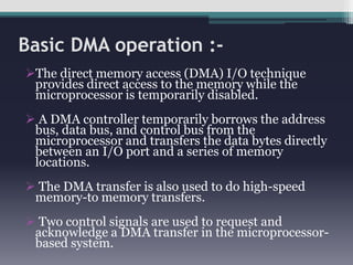


This presentation summarizes Direct Memory Access (DMA) and the Intel 8237 DMA controller. It defines DMA as transferring data between memory and I/O devices without CPU intervention, allowing high-speed transfers. The 8237 DMA controller handles DMA operations by controlling the address bus, data bus, and transfer modes. It has registers for addresses, counts, commands, modes and status. Transfer modes include single, block, demand, cascade and memory-to-memory.