Download as PDF, PPTX

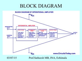
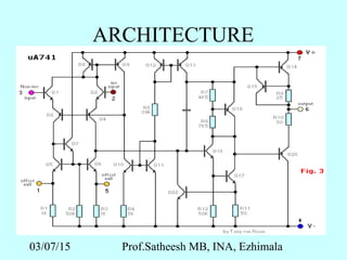
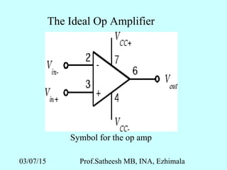
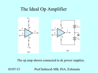
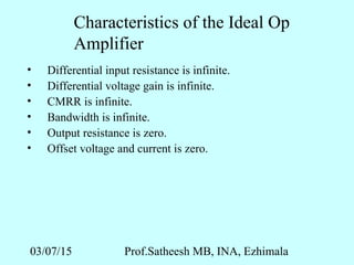
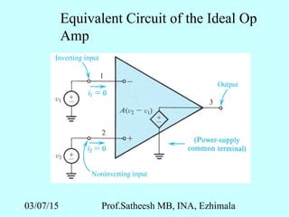
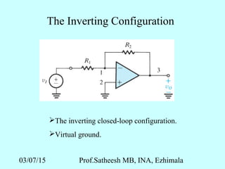
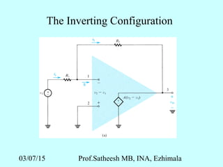
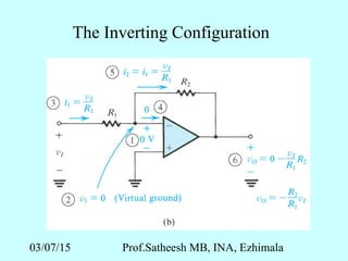
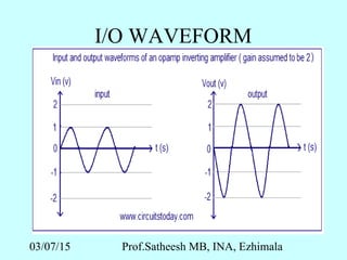
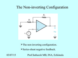
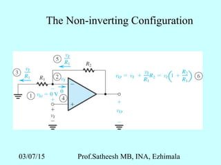
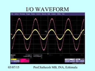
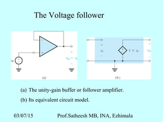
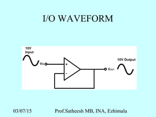
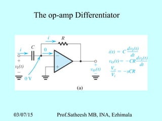
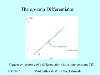
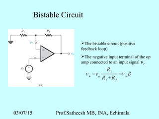
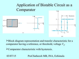
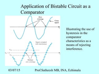
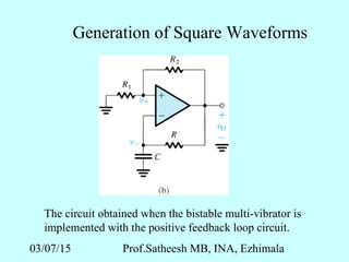

The document discusses operational amplifiers and their applications. It begins with an introduction to op amps and the 741 op amp circuit. It then describes the ideal op amp model and various op amp configurations like inverting, non-inverting, integrator, and differentiator. It also discusses bistable circuits and their application in comparators for generating square waves. The document contains circuit diagrams and descriptions of each op amp application.


![Acid rain powerpoint presentation[1]](https://cdn.slidesharecdn.com/ss_thumbnails/acidrainpowerpointpresentation1-130522105428-phpapp02-thumbnail.jpg?width=640&height=640&fit=bounds)