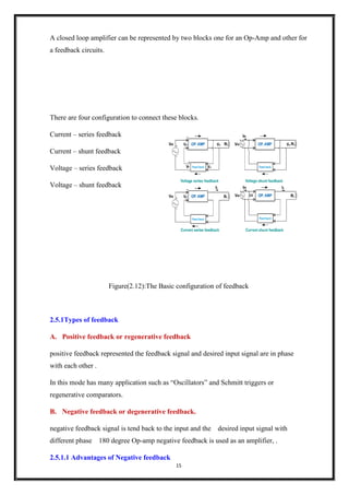
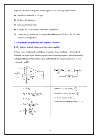
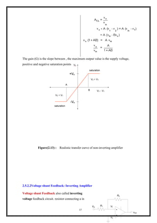
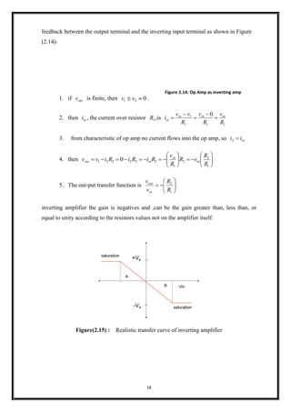
Download to read offline


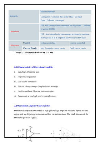
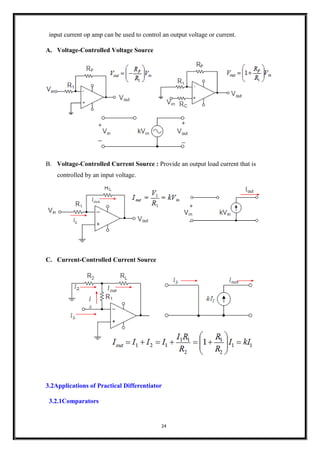
![10
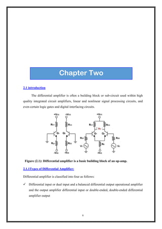
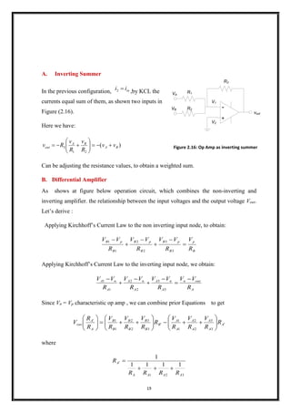
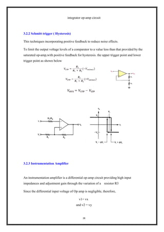
VO [Volts]
E+
E-
slope=A ≈ 200000
-Va
Va Vd = V+ - V-
[Volts]
Figure (2.4)block diagram of the Op amp
The two differential inputs V+ and V-one terminal output VO and VO is proportional to the
difference voltage Vd = V+ - V-. The DC voltages connected to operational amplifier
+Vcc and -Vcc (typically, +Vcc = 15 or 10 Volts and -Vcc = -15 or -10 Volts, respectively.) .
for input resistance is very large, the input currents I+ and I- are assumed negligibly small,
I+ = I- 0 A.
The transfer characteristics voltage of the Op-amp is plotted on Fig.
Figure (2.5)output-input voltage transfer characteristics of the Op Amp
The output VO is proportional to the difference signal Vd = V+ - V- in a very narrow range
(-Vcc < VO < Vcc) with Vcc and the gain there is A which is typically 40000.
there are different characteristics fin the market for several different operational
operational amplifier is uA741 general purpose used The top view of uA741 is given in
Fig(2.6)](https://image.slidesharecdn.com/opertionalamplifierkhirielrmalilibya-170816082746/85/Opertional-amplifier-khiri-elrmali-libya-10-320.jpg)

![39
Reference
[1] K.A. Connor, S. Bonner, P. Schoch Rensselaer Polytechnic Institute 8/16/2017
[2] Op Amp Mini-Tutorial Originally by Joydip Chakravarty,
[3] ELEK1289 - Electronic systems and practice II](https://image.slidesharecdn.com/opertionalamplifierkhirielrmalilibya-170816082746/85/Opertional-amplifier-khiri-elrmali-libya-39-320.jpg)

1) The document discusses operational amplifiers (Op-Amps), including their history, characteristics, and various configurations. 2) Op-Amps have very high gain, high input impedance, and low output impedance. They are often used in amplifier, filter, and instrumentation circuits. 3) There are two main Op-Amp configurations - open loop and closed loop. Open loop has stability issues while closed loop with negative feedback is more commonly used and has advantages like stabilized gain and reduced distortion. 4) Common closed loop Op-Amp circuits include the inverting amplifier, non-inverting amplifier, voltage follower, integrator, and differential amplifier. These are built using negative feedback techniques.


