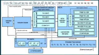
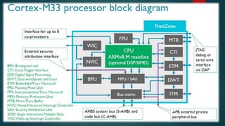
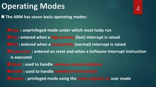
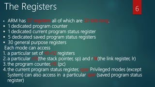
Aleppo University Computer Engineering Department Project
1. Aleppo University
Faculty of Electrical and Electronic Engineering
Computer Engineering Department
Supervised By:
PHD. Mohammed Ayman Naal
Prepared by:
Abdulrahman Haidar Mohammed Haj Hilal
Mohammed Hosam Diab
Second Semester
2017/2018
2. • Founded in November 1990
• Initial funding from Apple, Acorn and VLSI
• Designs the ARM range of RISC processor cores
Licenses ARM core designs to semiconductor
partners who fabricate and sell to their customers
• ARM does not fabricate silicon itself
• Also develop technologies to assist with the
designing of the ARM architecture
1. Software tools, boards, debug hardware
2. Application software
3. Bus architectures
4. Peripherals, etc
2
3. First ARM core (ARM1) ran code in April 1985…
3 stage pipeline very simple RISC-style processor
Original processor was designed for the Acorn Microcomputer
ARM Ltd formed in 1990 as an “Intellectual Property” company
Taking the 3 stage pipeline as the main building block
Code compatibility with ARM7TDMI remains very important
Especially at the applications level
The ARM architecture has features which derive from
ARM1
3
4. The ARM has seven basic operating modes:
User : unprivileged mode under which most tasks run
FIQ : entered when a high priority (fast) interrupt is raised
IRQ : entered when a low priority (normal) interrupt is raised
Supervisor : entered on reset and when a Software Interrupt instruction
is executed
Abort : used to handle memory access violations
Undef : used to handle undefined instructions
System : privileged mode using the same registers as user mode
4
6. ARM has 37 registers all of which are 32-bits long.
1 dedicated program counter
1 dedicated current program status register
5 dedicated saved program status registers
30 general purpose registers
Each mode can access
1. a particular set of r0-r12 registers
2. a particular r13(the stack pointer, sp) and r14(the link register, lr)
3. the program counter,r15 (pc)
4.the current program status register, cpsr Privileged modes (except
System) can also access in a particular spsr (saved program status
register)
6
8. When the processor is executing in ARM state:
All instructions are 32 bits wide
All instructions must be word aligned
Therefore the pc value is stored in bits [31:2] with bits [1:0] undefined (as instruction
cannot be halfword or byte aligned).
When the processor is executing in Thumb state:
All instructions are 16 bits wide
All instructions must be halfword aligned
Therefore the pc value is stored in bits [31:1] with bit [0] undefined (as instruction cannot
be byte aligned).
When the processor is executing in Jazelle state:
All instructions are 8 bits wide
Processor performs a word access to read 4 instructions at once
8
9. The Arm CPU architecture was originally based upon RISC (Reduced Instruction Set Computer)
principles.
A uniform register file, where instructions are not restricted to acting on specific registers.
A load/store architecture, where data processing operates only on register contents, not directly
on memory contents.
Simple addressing modes, where all load/store addresses are only determined from register contents and
instruction fields.
32-bit RISC architecture focused on core instruction set
Shifts available on data processing and address generation
Original architecture had 26-bit address space Augmented by a 32-bit address space early in the
evolution
Thumb instruction set was the next big step
9
10. There are three versions of the Arm architecture profile: A-, R- and M-
Profiles:
1. A-Profile is used in complex compute application areas,
such as servers, mobile phones and
automotive head units.
2. R-Profile is used where real-time response is required.
For example, safety critical applications or those needing a deterministic
response, such as medical equipment or vehicle steering, braking and
signaling.
3. M-Profile is used where energy efficiency, power conservation and size
are key.
M-Profile is especially suitable for deeply-embedded chips. For example,
in small sensors, communication modules and smart home products.
10
13. Key architecture revisions and products:
• ARMv1-ARMv3: largely lost in the mists of time
• ARMv4T: ARM7TDMI – first Thumb processor
• ARMv5TEJ(+VFPv2): ARM926EJ-S
• ARMv6K(+VFPv2): ARM1136JF-S, ARM1176JFZ-S, ARM11MPCore – first
Multiprocessing Core
• ARMv7-A+VFPv3 :Cortex-A8
• ARMv7-A+MPE+VFPv3: Cortex-A5, Cortex-A9
• ARMv7-A+MPE+VE+LPAE+VFPv4: Cortex-A15
• ARMv7-R : Cortex-R4, Cortex-R5
• ARMv6-M :Cortex–M0
• ARMv7-M: Cortex-M3, Cortex-M4
13
14. Architecture
core
bitwidth
Cores Holding
ARMv132ARM1
ARMv232
ARM2
ARM250
ARM3
ARMv332
ARM6
ARM7
ARMv432ARM8
ARMv4T32
ARM7TDMI
ARM9TDMI
SecurCore SC100
ARMv7E-M32
ARM Cortex-M4
ARM Cortex-M7
ARMv8-M32
ARM Cortex-M23
ARMCortex-M33
ARMv7-R32
ARM Cortex-R4
ARM Cortex-R5
ARM Cortex-R7
ARM Cortex-R8
Architecture
core
bitwidth
Cores Holding
ARMv8-R32ARM Cortex-R52
ARMv7-A32
ARM Cortex-A5
ARM Cortex-A7
ARM Cortex-A8
ARM Cortex-A9
ARM Cortex-A12
ARM Cortex-A15
ARM Cortex-A17
ARMv8-A32ARM Cortex-A32
ARMv8-A64/32
ARM Cortex-A35
ARM Cortex-A53
ARM Cortex-A57
ARM Cortex-A72
ARM Cortex-A73
ARMv8.1-A64/32TBA
ARMv8.2-A64/32
ARM Cortex-A55
ARM Cortex-A75
ARMv8.3-A64/32TBA
ARMv8.4-A64/32TBA
14
17. • The ARM7TDMI processor has two instruction
sets:
1- the 32-bit ARM instruction set
2- the 16-bit Thumb instruction set.
• Simple 3 stage pipeline Fetch, Decode, Execute
• Multiple cycles in execute stage for Loads/Stores
• Simple core
17ARMv7TDMI
19. ARMv5TEJ introduced:
• Better interworking between ARM and Thumb
• Bottom bit of the address used to determine
the ISA
• Jazelle-DBX for Java byte code interpretation
in hardware
19
20. • 5 stage pipeline single issue core
Fetch, Decode, Execute, Memory, Writeback
• Most common instructions take 1 cycle in each
pipeline stage
• Split Instruction/Data Level1 caches Virtually
tagged
• MMU – hardware page table walk based
20ARM926EJ-S
21. • 8 stage pipeline single issue
• Split Instruction/Data Level1 caches Physically tagged
• Two cycle memory latency
• MMU – hardware page table walk based
• Hardware branch prediction
21
24. • high-performance, low-power, cached application processor that provides full virtual memory
capabilities
• 10 stage pipeline (+ Neon Engine)
• 2 levels of cache – L1 I/D split, L2 unified
• configurable 64-bit or 128-bit high-speed Advanced Microprocessor Bus Architecture (AMBA)
• a NEON pipeline for executing Advanced SIMD and VFP instruction sets
• Aggressive, dynamic branch prediction with branch target address cache, global history buffer, and
8-entry return stack
• Memory Management Unit (MMU) and separate instruction and data Translation Look-aside Buffers
(TLBs) of 32 entries each
• Level 1 instruction and data caches of 16KB or 32KB configurable size
• Level 2 cache of 128KB through 1MB configurable size
• Level 2 cache with parity and Error Correction Code (ECC) configuration option
• Embedded Trace Macro cell (ETM) support for non-invasive debug
• static and dynamic power management including Intelligent Energy Management
(IEM)
24
25. • MP capable – delivered as clusters of 1 to 4 CPUs
• MESI based coherency scheme across L1 data caches
• Shared L2 cache (PL310)
• Integrated interrupt controller
25
26. • 2.5 Ghz in 28 HP process
12 stage in-order, 3-12 stage OoO pipeline
• 3.5 DMIPS/Mhz ~ 8750 DMIPS @ 2.5GHz
• Dynamic repartition Virtualization
• Fast state save and restore
• Move execution between cores/clusters
• 128-bit AMBA 4 ACE bus
• Supports system coherency
• ECC on L1 and L2 caches
26
27. 27
Rich, unified Thumb-2 high performance instruction set
Smallest code size and reduced memory requirements
Fast MAC support
Accelerated bit-field processing
Harvard architecture:
Allows simultaneous code and data access
Reduce interrupt latency
Fully configurable to balance features and silicon area
Low latency, integrated Nested Vectored Interrupt Controller (NVIC) Sophisticated debug
and trace support
Memory Protection Unit (MPU)
Embedded Trace Macrocell (ETM)