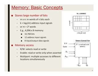
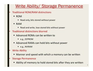
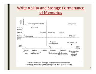
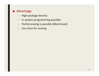
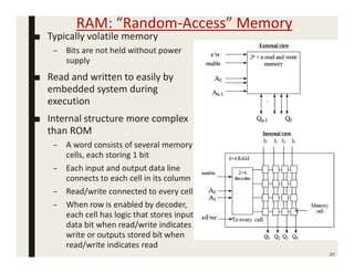
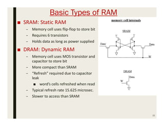
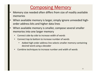
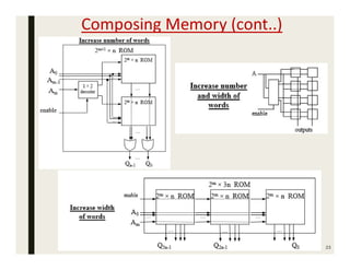
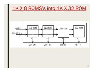
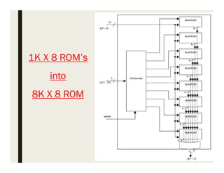
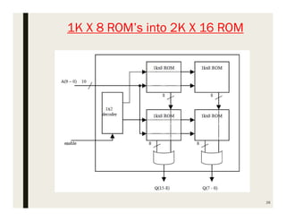
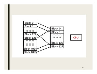
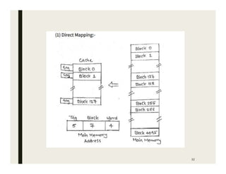
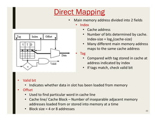
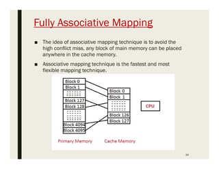
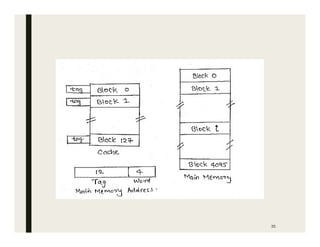
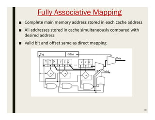
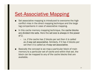
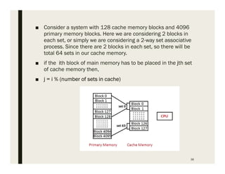
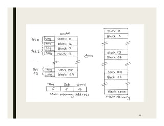
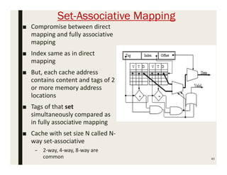
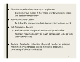
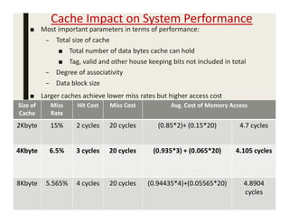
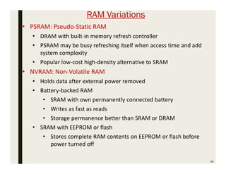
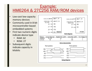
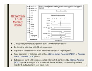
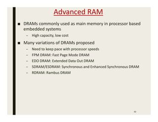
MODULE – 3
Memory Design
1
Chapter Summary
2
■ Memory devices used in microcontroller based embedded
systems
■ Timing diagrams – Read and write operations
■ Burst read/write devices
■ Composing Memory
■ Cache Design
– Cache Mapping and Replacement Policies
– Cache Write Techniques
■ Basic Protocol Concepts
■ ISA Bus Protocol
■ Serial Protocols
■ Parallel Protocols
Memory: Basic Concepts
■ Stores large number of bits
– m x n: m words of n bits each
– k = log2(m) address input signals
– or m = 2k words
– E.g., 4,096 x 8 memory:
■ 32,768 bits
■ 12 address input signals
■ 8 input/output data signals
■ Memory access
– R/W: selects read or write
– Enable: read or write only when asserted
– Multiport: multiple accesses to different
locations simultaneously
3
Write Ability/ Storage Permanence
4
• Traditional ROM/RAM distinctions
 ROM
 Read only, bits stored without power
 RAM
 Read and write, lose stored bits without power
• Traditional distinctions blurred
 Advanced ROMs can be written to
 e.g., EEPROM
 Advanced RAMs can hold bits without power
 e.g., NVRAM
• Write Ability
 Manner and speed with which a memory can be written
• Storage Permanence
 Ability of memory to hold stored bits after they are written
Write Ability and Storage Permenance
of Memories
5
Write Ability
■ Ranges of write ability
– High end
■ processor writes to memory simply and quickly
■ e.g., RAM
– Middle range
■ processor writes to memory, but slower
■ e.g., FLASH, EEPROM
– Lower range
■ special equipment, “programmer”, must be used to write to
memory
■ e.g., EPROM, OTP ROM
– Low end
■ bits stored only during fabrication
■ e.g., Mask-programmed ROM
■ In-system programmable memory
– Can be written to by a processor in the embedded system using the
memory
– Memories in high end and middle range of write ability 6
Storage Permanence
■ Range of Storage Permanence
– High End
■ Essentially never loses bits
■ e.g., mask-programmed ROM
– Middle Range
■ Holds bits days, months, or years after memory’s power source
turned off
■ e.g., NVRAM
– Lower Range
■ Holds bits as long as power supplied to memory
■ e.g., SRAM
– Low End
■ Begins to lose bits almost immediately after written
■ e.g., DRAM
■ Non-Volatile Memory
– Holds bits even after power is no longer supplied
– High end and middle range of storage permanence 7
ROM: “Read-Only” Memory
8
■ Nonvolatile memory
■ Can be read from but not written
to, by a processor in an embedded
system
■ Traditionally written to,
“programmed”, before inserting
to embedded system
■ Uses
– Store software program for general-
purpose processor
■ program instructions can be one or
more ROM words
– Store constant data needed by
system
– Implement combinational circuit
Example: 8 x 4 ROM
■ Horizontal lines = words
■ Vertical lines = data
■ Lines connected only at
circles
■ Decoder sets word 2’s line to
1 if address input is 010
■ Data lines Q3 and Q1 are set
to 1 because there is a
“programmed” connection
with word 2’s line
■ Word 2 is not connected with
data lines Q2 and Q0
■ Output is 1010
9
Implementing Combinational Function
■ Any combinational circuit of n functions of same k variables can
be done with 2k x n ROM
10x
Mask-Programmed ROM
11
■ Connections “programmed” at fabrication
– Set of masks
■ Lowest write ability
– Only once it can be programmed
■ Highest storage permanence
– Bits never change unless damaged
■ Typically used for final design of high-volume systems
– Spread out NRE cost for a low unit cost
OTP ROM: One-time Programmable ROM
■ Connections “programmed” after manufacture by user
– User provides file of desired contents of ROM
– File input to machine called ROM programmer
– Each programmable connection is a fuse
– ROM programmer blows fuses where connections should
not exist
■ Very low write ability
– Typically written only once and requires ROM programmer
device
■ Very high storage permanence
– Bits don’t change unless reconnected to programmer and
more fuses blown
■ Commonly used in final products
– Cheaper, harder to inadvertently modify 12
EPROM: Erasable Programmable ROM
13
• Programmable component is a MOS transistor
• Transistor has “floating” gate surrounded by an insulator
• (a) Negative charges form a channel between source and drain storing a
logic 1
• (b) Large positive voltage at gate causes negative charges to move out of
channel and get trapped in floating gate storing a logic 0
• (c) (Erase) Shining UV rays on surface of floating-gate causes negative
charges to return to channel from floating gate restoring the logic 1
• (d) An EPROM package showing quartz window through which UV light can
pass
• Better write ability
• Can be erased and reprogrammed thousands of times
• Reduced storage permanence
• Program lasts about 10 years but is susceptible to radiation and electric
noise
• Typically used during design development
EPROM
14
■ Advantage
– High package density (1MOSFET/bit)
■ Drawbacks
– Erasing takes more time (UV light exposure)
– Not in system programmable
– Partial erasing is not possible
15
EEPROM: Electrically Erasable Programmable ROM
■ Programmed and erased electronically
– Can program and erase individual words
– Programmed by applying positive gate pulse
– Erased by applying the negative of same pulse
■ Difference from EPROM
– Floating gate MOSFET – SiO2 thickness is less
– Less gate voltage required to trap electrons
■ Better write ability
– Can be in-system programmable with built-in circuit to provide higher than
normal voltage
■ Built-in memory controller commonly used to hide details from memory user
– Writes very slow due to erasing and programming
■ “Busy” pin indicates to processor EEPROM still writing
– Can be erased and programmed tens of thousands of times
■ Similar storage permanence to EPROM (about 10 years)
■ Far more convenient than EPROMs, but more expensive
16
■ Advantage
– Erasing takes place at a faster rate
– In system programming is possible
– Partial erasing is possible
■ Drawbacks
– Low package density (2 MOSFET’s / bit – 1 for
selecting each bit for erasing)
– High cost per bit
17
Flash Memory
18
■ Extension of EEPROM
– Same floating gate principle
– Same write ability and storage permanence
■ Fast erase
– Large blocks of memory erased at once, rather than one word at a
time
– Blocks typically several thousand bytes large
■ Writes to single words may be slower
– Entire block must be read, word updated, then entire block written
back
■ Used with embedded systems storing large data items in
nonvolatile memory
– e.g., digital cameras, TV set-top boxes, cell phones
■ Advantage
– High package density
– In system programming possible
– Partial erasing is possible (Block level)
– Less time for erasing
19
RAM: “Random-Access” Memory
■ Typically volatile memory
– Bits are not held without power
supply
■ Read and written to easily by
embedded system during
execution
■ Internal structure more complex
than ROM
– A word consists of several memory
cells, each storing 1 bit
– Each input and output data line
connects to each cell in its column
– Read/write connected to every cell
– When row is enabled by decoder,
each cell has logic that stores input
data bit when read/write indicates
write or outputs stored bit when
read/write indicates read
20
Basic Types of RAM
■ SRAM: Static RAM
– Memory cell uses flip-flop to store bit
– Requires 6 transistors
– Holds data as long as power supplied
■ DRAM: Dynamic RAM
– Memory cell uses MOS transistor and
capacitor to store bit
– More compact than SRAM
– “Refresh” required due to capacitor
leak
■ word’s cells refreshed when read
– Typical refresh rate 15.625 microsec.
– Slower to access than SRAM
21
Composing Memory
22
• Memory size needed often differs from size of readily available
memories
• When available memory is larger, simply ignore unneeded high-
order address bits and higher data lines
• When available memory is smaller, compose several smaller
memories into one larger memory
• Connect side-by-side to increase width of words
• Connect top to bottom to increase number of words
• Added high-order address line selects smaller memory containing
desired word using a decoder
• Combine techniques to increase number and width of words
Composing Memory (cont..)
23
1K X 8 ROMS’s into 1K X 32 ROM
24
25
1K X 8 ROM’s
into
8K X 8 ROM
26
1K X 8 ROM’s into 2K X 16 ROM
Memory Hierarchy
■ Want inexpensive, fast memory Inexpensive memory slow ; Fast
memory expensive
■ Main Memory
– Inexpensive, slow memory stores entire program and data
■ Cache
– Small, expensive, fast memory stores copy of likely accessed parts of larger
memory
– Can be multiple levels of cache
27
Cache Memory
■ Usually designed with SRAM, rather than DRAM
– More expensive but faster than main memory
■ Usually on same chip as processor
– Space limited, so much smaller than off-chip main memory
– Faster access ( 1 cycle vs. several cycles for main memory)
■ Cache operation:
– Request for main memory access (read or write)
– First, check cache for copy
■ Cache hit
– Copy is in cache, quick access
■ Cache miss
– Copy not in cache, read address and possibly its neighbors into
cache
■ Several cache design choices
– Cache mapping, replacement policies, and write techniques
28
Cache Mapping
■ Method for assigning main memory address to the far fewer
number of available cache addresses
■ To determine whether a particular main memory address
contents are in the cache
■ Three basic techniques:
– Direct mapping
– Fully associative mapping
– Set-associative mapping
■ Caches partitioned into indivisible blocks or lines of adjacent
memory addresses
– usually 4 or 8 addresses per line
29
Direct Mapping:
■ The direct mapping concept is if the ith block of main memory
has to be placed at the jth block of cache memory then, the
mapping is defined as:
 j = i % (number of blocks in cache memory)
■ Suppose, there are 4096 blocks in primary memory and 128
blocks in the cache memory.
■ Then the situation is like, the 0th block of main memory into
the cache memory, then apply the above formula.
 0 % 128 = 0
■ Similarly, the 1st block of main memory will be mapped to the
1st block of cache, then 2nd block to 2nd block of the cache
and so on.
■ So, this is how direct mapping in the cache memory is done.
The following diagram illustrates the direct mapping process.
30
31
32
Direct Mapping
33
• Main memory address divided into 2 fields
• Index
• Cache address
• Number of bits determined by cache.
Index-size = log2(cache-size)
• Many different main memory address
maps to the same cache address
• Tag
• Compared with tag stored in cache at
address indicated by index
• If tags match, check valid bit
• Valid bit
• Indicates whether data in slot has been loaded from memory
• Offset
• Used to find particular word in cache line
• Cache line/ Cache Block – Number of inseparable adjacent memory
addresses loaded from or stored into memory at a time
• Block size = 4 or 8 addresses
Fully Associative Mapping
■ The idea of associative mapping technique is to avoid the
high conflict miss, any block of main memory can be placed
anywhere in the cache memory.
■ Associative mapping technique is the fastest and most
flexible mapping technique.
34
35
Fully Associative Mapping
■ Complete main memory address stored in each cache address
■ All addresses stored in cache simultaneously compared with
desired address
■ Valid bit and offset same as direct mapping
36
Set-Associative Mapping
■ Set associative mapping is introduced to overcome the high
conflict miss in the direct mapping technique and the large
tag comparisons in case of associative mapping.
■ In this cache memory mapping technique, the cache blocks
are divided into sets. Here the set size is always in the power
of 2,
– i.e. if the cache has 2 blocks per set then it is called
as 2-way set associative. Similarly, if it has 4 blocks per
set then it is called as 4-way set associative.
■ Basically the concept is we map a particular block of main
memory to a particular set of cache and within that set, the
block can be mapped to any of the cache blocks that are
available.
37
■ Consider a system with 128 cache memory blocks and 4096
primary memory blocks. Here we are considering 2 blocks in
each set, or simply we are considering a 2-way set associative
process. Since there are 2 blocks in each set, so there will be
total 64 sets in our cache memory.
■ if the ith block of main memory has to be placed in the jth set
of cache memory then,
■ j = i % (number of sets in cache)
38
39
Set-Associative Mapping
■ Compromise between direct
mapping and fully associative
mapping
■ Index same as in direct
mapping
■ But, each cache address
contains content and tags of 2
or more memory address
locations
■ Tags of that set
simultaneously compared as
in fully associative mapping
■ Cache with set size N called N-
way set-associative
– 2-way, 4-way, 8-way are
common 40
41
■ Direct Mapped caches are easy to implement
– But numerous misses if 2 or more words with same index
are accessed frequently
■ Fully Associative Caches
– Fast, but the comparison logic is expensive to implement
■ Set Associative Caches
– Reduce misses compared to direct mapped caches
– Without requiring nearly as much comparison logic as fully
associative cache
■ Caches – Treated as collection of a small number of adjacent
main memory addresses as one indivisible block/line –
Consisting of about 8 addresses
Cache-Replacement Policy
42
• Technique for choosing which block to replace
• When fully associative cache is full
• When set-associative cache’s line is full
• Direct mapped cache has no choice
• Main memory address always maps to the same cache address and
replaces whatever block is already there.
• Random
• Replace block chosen at random
• Does nothing to prevent replacing a block i.e., likely to be used again soon
• LRU: least-recently used
• Replace block not accessed for longest time
• Means that it is least likely to be used in near future
• Excellent hit/miss ratio but requires expensive hardware
• FIFO: first-in-first-out
• Push block onto queue when accessed
• Choose block to replace by popping queue
Cache Write Techniques
■ When written, data cache must update main memory
■ Write-through
– Write to main memory whenever cache is written to
– Easiest to implement
– Processor must wait for slower main memory write
– Potential for unnecessary writes
■ Write-back
– Reduces number of writes to main memory by writing a block into main
memory only when block is replaced
– Extra dirty bit for each block set when cache block written to
– Check dirty bit while replacing the block to determine whether we
should copy the block to main memory
43
Cache Impact on System Performance
■ Most important parameters in terms of performance:
– Total size of cache
■ Total number of data bytes cache can hold
■ Tag, valid and other house keeping bits not included in total
– Degree of associativity
– Data block size
■ Larger caches achieve lower miss rates but higher access cost
44
Size of
Cache
Miss
Rate
Hit Cost Miss Cost Avg. Cost of Memory Access
2Kbyte 15% 2 cycles 20 cycles (0.85*2)+ (0.15*20) 4.7 cycles
4Kbyte 6.5% 3 cycles 20 cycles (0.935*3) + (0.065*20) 4.105 cycles
8Kbyte 5.565% 4 cycles 20 cycles (0.94435*4)+(0.05565*20) 4.8904
cycles
Cache Performance Trade-offs
■ Increasing size
– Additional access time penalty
■ Improving cache hit rate without increasing size
– Increase line size
■ Improves main memory access time, at the expense of more
complex multiplexing of data and thus increased access latency
– Change set-associativity
– Both incur additional logic and add to access time latency
45
RAM Variations
46
• PSRAM: Pseudo-Static RAM
• DRAM with built-in memory refresh controller
• PSRAM may be busy refreshing itself when access time and add
system complexity
• Popular low-cost high-density alternative to SRAM
• NVRAM: Non-Volatile RAM
• Holds data after external power removed
• Battery-backed RAM
• SRAM with own permanently connected battery
• Writes as fast as reads
• Storage permanence better than SRAM or DRAM
• SRAM with EEPROM or flash
• Stores complete RAM contents on EEPROM or flash before
power turned off
47
Example:
HM6264 & 27C256 RAM/ROM devices
• Low-cost low-capacity
memory devices
• Commonly used in 8-bit
microcontroller-based
embedded systems
• First two numeric digits
indicate device type
• RAM: 62
• ROM: 27
• Subsequent digits
indicate capacity in
kilobits
TC55V2325
FF-100
Memory
Device
48
■ 2-megabit synchronous pipelined burst SRAM memory device
■ Designed to interface with 32-bit processors
■ Capable of fast sequential reads and writes as well as single byte I/O
■ Read operation  Initiated with either Address Status Processor (ADSP) or Address
Status Controller (ADSC) input
■ Subsequent burst addresses generated internally & controlled by Address Advance
(ADV) input As long as ADV is asserted, device will keep incrementing address
register & output data in next clock cycle
Advanced RAM
■ DRAMs commonly used as main memory in processor based
embedded systems
– High capacity, low cost
■ Many variations of DRAMs proposed
– Need to keep pace with processor speeds
– FPM DRAM: Fast Page Mode DRAM
– EDO DRAM: Extended Data Out DRAM
– SDRAM/ESDRAM: Synchronous and Enhanced Synchronous DRAM
– RDRAM: Rambus DRAM
49
Basic DRAM
50
• Address bus multiplexed between row and column components
• Row and column addresses are latched in, sequentially, by
strobing ‘ras’ and ‘cas’ signals, respectively
• Refresh circuitry can be external or internal to DRAM device
• Strobes consecutive memory address periodically causing memory
content to be refreshed
• Refresh circuitry disabled during read or write operation
Fast Page Mode DRAM (FPM DRAM)
51
■ Each row of memory bit array is viewed as a page
■ Page contains multiple words
■ Individual words addressed by column address
■ Timing diagram:
– row (page) address sent
– 3 words read consecutively by sending column address for each
■ Extra cycle eliminated on each read/write of words from same
page
Extended data out DRAM (EDO DRAM)
■ Improvement of FPM DRAM
■ Extra latch before output buffer
– Allows strobing of cas before data read operation completed
■ Reduces read/write latency
52
(S)ynchronous and
Enhanced Synchronous (ES) DRAM
■ SDRAM latches data on active edge of clock
■ Eliminates time to detect ras/cas and rd/wr signals
■ A counter is initialized to column address then incremented on
active edge of clock to access consecutive memory locations
■ ESDRAM improves SDRAM
– Added buffers enable overlapping of column addressing
– Faster clocking and lower read/write latency possible
53
Rambus DRAM (RDRAM)
■ More of a bus interface architecture than DRAM architecture
■ Uses multiplexed address/data lines to connect the memory
controller/processor to RDRAM
■ Clock runs at 300MHz
■ Data is latched on both rising and falling edge of clock
■ Broken into 4 banks each with own row decoder
– Can have 4 pages open at a time
■ Packet driven – Address packets followed by data packets
■ Smallest transaction requires a minimum of 4 cycles
■ Multiple open page schemes & fast bus I/O
– Capable of very high throughput
54
DRAM Integration Problem
55
■ SRAM easily integrated on same chip as processor
■ DRAM more difficult
– Different chip making process between DRAM and
conventional logic
– Goal of conventional logic (IC) designers:
■ Minimize parasitic capacitance to reduce signal propagation
delays and power consumption
– Goal of DRAM designers:
■ Create capacitor cells to retain stored information
– Difference in design goals leads to a design process i.e.,
considerably different in DRAM and conventional IC’s.
Memory Management Unit (MMU)
56
• Duties of MMU
• Handles DRAM refresh, bus interface and arbitration
• Takes care of memory sharing among multiple processors
• Translates logic memory addresses from processor to physical
memory addresses of DRAM
• Modern CPUs often come with MMU built-in
• Single-purpose processors can be designed or purchased to
handle memory management tasks
Introduction to Protocols
■ Embedded system functionality aspects
– Processing
■ Transformation of data
■ Implemented using processors
– Storage
■ Data Control
■ Implemented using memory
– Communication
■ Transfer of data between processors and memories
■ Implemented using buses
■ Called interfacing
57
A Simple Bus
■ Wires:
– Uni-directional or bi-
directional
■ Bus
– Set of wires with a single
function
■ Address bus, data bus
– Associated protocol: rules for
communication
58
Ports
■ Conducting device on periphery
■ Connects bus to processor or
memory
■ Often referred to as a pin
– Actual pins on periphery of IC
package that plug into socket on
printed-circuit board
– Sometimes metallic balls instead
of pins
– Today, metal “pads” connecting
processors and memories within
single IC
■ Single wire or set of wires with
single function
– E.g., 12-wire address port
59
Timing Diagrams
60
■ Most common method for describing a
communication protocol
■ Time proceeds to the right on x-axis
■ Control signal: low or high
– May be active low (e.g., go’ or go or
go_L)
– Use terms assert (active) and de-
assert
– Asserting go’ means go=0
■ Data signal: not valid or valid
■ Protocol may have sub-protocols
– Called bus cycle, e.g., read and write
– Each may be several clock cycles
■ Read example
– rd’/wr set low, address placed on addr
for at least tsetup time before enable
asserted, enable triggers memory to
place data on data wires by time tread
Basic Protocol Concepts
■ Actor: master initiates, servant (slave) respond
■ Direction: sender, receiver
■ Addresses: special kind of data
– Specifies a location in memory, a peripheral, or a register within a
peripheral
■ Time multiplexing
– Share a single set of wires for multiple pieces of data
– Saves wires at expense of time
61
Basic Protocol Concepts: Control Methods
62
A Strobe/Handshake Compromise
63
Parallel Communication
■ Multiple bits of data, in addition to control, and possibly
power wires
– One bit per wire
■ High data throughput for short distances
■ Typically used when connecting devices on same IC or same
circuit board
– Bus must be kept short
■ Long parallel wires result in high capacitance values which
requires more time to charge/discharge
■ Small variations in the length of individual wires of parallel bus
can cause received bits to arrive at different times
■ Higher cost, bulky
– Especially when considering the insulation that must be
used to prevent the noise from each wire from interfering
with other wires
64
Serial Communication
■ Single data wire, possibly also control and power wires
■ Words transmitted one bit at a time
■ Higher data throughput with long distances
– Less average capacitance, so more bits per unit of time
■ Cheaper to build since it has few wires
■ More complex interfacing logic and communication protocol
– Sender needs to decompose word into bits
– Receiver needs to recompose bits into word
– Control signals often sent on same wire as data - Increases protocol
complexity
65
66
• Most serial bus protocols eliminate the need for extra control
signals – Read and write – By using the same wire that carries
data for the R/W purpose
• When data is to be sent
• First transmits a start bit
• Signals the receiver to wakeup and start receiving data
• Followed by N data bits and a stop bit.
• Stop bits – Signals the receiver the end of the transmission
• Transmitter and Receiver agree upon a pre-determined
transmission speed
• After seeing a start bit, receiver simply samples data at
predetermined frequency until all N bits are received
• Common Synchronization – Use an additional wire for clocking
purpose
Serial Protocols: I2C
■ I2C (Inter-IC)
– Two-wire serial bus protocol developed by Philips
Semiconductors nearly 20 years ago
– Enables peripheral IC’s to communicate using simple
communication hardware
– Data transfer rates up to 100 kbits/s and 7-bit addressing
possible in normal mode
– 7-bit addressing  128 devices can be communicate
– Recently enhanced to include fast mode: 3.4 Mbits/s and
10-bit addressing in fast-mode
– Common devices capable of interfacing to I2C bus:
■ EPROMS, Flash, and some RAM memory, real-time clocks,
watchdog timers, and microcontrollers
67
I2C Bus Structure
68
69
• Bus consists of 2 wires – Serial Data Line (SDL) and Serial Clock
Line (SCL)
• Doesn’t limit the length of bus wires, as long as the total
capacitance of the bus remains under 400pF.
• Operation
• Master initiates the data transfer - Does not limit the number of
master devices
• Both master and slave can be senders or receivers of data
• Start Condition – High to Low on SDA line; High on SCL
• Stop Condition – Low to high on SDA line; High on SCL
• Master initiates the data transfer by a start condition – Address
starting from MSB to LSB
• Bit value is placed on SDA line
• Write operation – After sending a data, master sends a zero
• Receiver returns the acknowledgement by returning a low
Serial Protocols: USB
■ USB (Universal Serial Bus)
– Easier connection between PC and monitors, printers, digital
speakers, modems, scanners, digital cameras, joysticks,
multimedia game equipment
– 2 data rates:
■ 12 Mbps for increased bandwidth devices
■ 1.5 Mbps for lower-speed devices (joysticks, game pads)
70
• Tiered star topology can be used
• One USB device (hub) connected
to PC
• Hub can be embedded in devices
like monitor, printer, or keyboard
or can be standalone
• Only 1 device needs to be plugged
into PC, others can be connected
to host
71
• Hubs – Upstream connection towards PC as well as multiple
downstream ports to allow the connection of additional peripheral
devices Up to 127 devices can be connected like this
• USB host controller
• Manages and controls bandwidth and driver software required by
each peripheral
• Users don’t need to do anything, because all the configuration
steps happen automatically
• Allocates electrical power to USB devices
• USB hubs
• Detect attachments and detachments of peripherals occurring
downstream
• Dynamically allocates power downstream according to devices
connected/disconnected
• Power is distributed through USB cables, max. length of 5m –
Not a big AC power supply box is required for many devices
Serial Protocols: CAN
■ CAN (Controller area network)
– Protocol for real-time applications carried over a twisted pair of
wires
– Developed by Robert Bosch GmbH
– Originally for communication among components of cars
– Applications now using CAN include:
■ Elevator controllers, copiers, telescopes, production-line
control systems, and medical instruments
– Data transfer rates up to 1 Mbit/s
– 11-bit addressing
– Error detection capabilities
– Documented in ISO 11898 (for high speed applications) and ISO
11519-2 (for low speed applications)
72
73
• Common devices interfacing with CAN:
• 8051-compatible 8592 processor and standalone CAN
controllers such as 80C200 from Philips
• Actual physical design of CAN bus not specified in protocol
• Requires devices to transmit/detect dominant and recessive
signals to/from bus
• e.g., ‘1’ = dominant, ‘0’ = recessive if single data wire used
• Bus guarantees dominant signal prevails over recessive signal if
asserted simultaneously
Serial Protocols: FireWire
■ FireWire (a.k.a. I-Link, Lynx, IEEE 1394)
– High-performance serial bus developed by Apple Computer
Inc.
– Need for FireWire - Rapidly growing need for mass
information transfer
– Typical LAN’s/WAN’s
■ Incapable of providing cost effective connection capabilities
■ Do not guarantee bandwidth for real time applications
– Data transfer rates from 12.5 to 400 Mbits/s, 64-bit
addressing
– Real time connection/disconnect & address assignment 
Plug-and-play capability
– Packet-based layered design structure
74
75
• Designed for interfacing independent electronic components (I2C
and CAN – used for interfacing IC’s)
e.g., Desktop Computer, Digital Scanner
• Capable of supporting a LAN similar to Ethernet
• 64-bit address:
• 10 bits for network identifiers, 1023 subnetworks
• 6 bits for node identifiers, each subnetwork can have 63
nodes
• 48 bits for memory address, each node can have 281
terabytes of distinct locations
• Applications using FireWire include:
• Disk drives, Printers, Scanners, Cameras and other consumer
electronic devices
Parallel Protocols: PCI Bus
■ PCI Bus (Peripheral Component Interconnect)
– High performance bus originated at Intel in the early 1990’s
– Standard adopted by industry and administered by PCISIG (PCI
Special Interest Group)
– Interconnects chips, expansion boards, processor memory
subsystems
– First used in personal computers in 1994 with Intel 486 processors
– Data transfer rates of 127.2 to 508.6 Mbits/s and 32-bit addressing
■ Later extended to 64-bit while maintaining compatibility with
32-bit schemes
– Synchronous bus architecture
– Multiplexed data/address lines
– Replaced the ISA/EISA architecture and Micro-Channel bus
protocols
76
77
■ PCI driver can access hardware automatically as well as address
assigned by the programmer
■ PCI feature – Automatically detecting the interfacing systems and
assigning new addresses – Important for coding a device driver
– Simplifies the addition and deletion of system peripherals
Parallel Protocols: ARM Bus
■ ARM Bus
– PCI is widely used industry standards – many other bus
protocols are predominantly designed and used internally
by various IC design companies
– Designed and used internally by ARM Corporation
– Interfaces with ARM line of processors
– Synchronous data transfer architecture
– Many IC design companies have own bus protocol
– Data transfer rate is a function of clock speed
■ If clock speed of bus is X, transfer rate = 16*X bits/s
– 32-bit addressing
78
ISA Bus Protocol – Memory Access
■ ISA: Industry Standard
Architecture
– Common in 80x86’s
■ Features
– 20-bit address
– Compromise
strobe/handshake
control
■ 4 cycles default
■ Unless CHRDY
deasserted –
resulting in
additional wait
cycles (up to 6)
79
Microprocessor Interfacing: I/O Addressing
■ A microprocessor communicates with other devices
using some of its pins
– Port-based I/O (parallel I/O)
■ Processor has one or more N-bit ports
■ Processor’s software reads and writes a port just like a
register
■ E.g., P0 = 0xFF; v = P1.2; -- P0 and P1 are 8-bit ports
– Bus-based I/O
■ Processor has address, data and control ports that form a
single bus
■ Communication protocol is built into the processor
■ A single instruction carries out the read or write protocol
on the bus
80
Compromises/Extensions
81
• Parallel I/O peripheral
• When processor only supports bus-
based I/O but parallel I/O needed
• Each port on peripheral connected to a
register within peripheral that is
read/written by the processor
• Extended parallel I/O
• When processor supports port-based
I/O but more ports needed
• One or more processor ports interface
with parallel I/O peripheral extending
total number of ports available for I/O
• e.g., extending 4 ports to 6 ports in
figure
Types of Bus-based I/O:
Memory-Mapped I/O and Standard I/O
82
■ Processor talks to both memory and peripherals using same bus –
two ways to talk to peripherals
– Memory-mapped I/O
■ Peripheral registers occupy addresses in same address space as
memory
■ e.g., Bus has 16-bit address
– lower 32K addresses may correspond to memory
– upper 32k addresses may correspond to peripherals
– Standard I/O (I/O-mapped I/O)
■ Additional pin (M/IO) on bus indicates whether a memory or
peripheral access
■ e.g., Bus has 16-bit address
– all 64K addresses correspond to memory when M/IO set to 0
– all 64K addresses correspond to peripherals when M/IO set to 1
Memory-mapped I/O vs. Standard I/O
83
■ Memory-mapped I/O
– Requires no special instructions
■ Assembly instructions involving memory like MOV and ADD work
with peripherals as well
■ Standard I/O requires special instructions (e.g., IN, OUT) to move
data between peripheral registers and memory
■ Standard I/O
– No loss of memory addresses to peripherals
– Simpler address decoding logic in peripherals possible
■ When number of peripherals much smaller than address space then
high-order address bits can be ignored
– smaller and/or faster comparators
ISA Bus Protocol – Standard I/O
84
■ ISA supports standard I/O
– /IOR distinct from /MEMR for peripheral read
■ /IOW used for writes
– 16-bit address space for I/O vs. 20-bit address space for
memory
– Otherwise very similar to memory protocol
ISA bus DMA cycles
85
• R – DMA Request
• A – DMA Acknowledge
Serial Protocols: FireWire
■ FireWire (a.k.a. I-Link, Lynx, IEEE 1394)
– High-performance serial bus developed by Apple Computer
Inc.
– Need for FireWire - Rapidly growing need for mass
information transfer
– Typical LAN’s/WAN’s
■ Incapable of providing cost effective connection capabilities
■ Do not guarantee bandwidth for real time applications
– Data transfer rates from 12.5 to 400 Mbits/s, 64-bit
addressing
– Real time connection/disconnect & address assignment 
Plug-and-play capability
– Packet-based layered design structure
86
87
• Designed for interfacing independent electronic components (I2C
and CAN – used for interfacing IC’s)
e.g., Desktop Computer, Digital Scanner
• Capable of supporting a LAN similar to Ethernet
• 64-bit address:
• 10 bits for network identifiers, 1023 subnetworks
• 6 bits for node identifiers, each subnetwork can have 63
nodes
• 48 bits for memory address, each node can have 281
terabytes of distinct locations
• Applications using FireWire include:
• Disk drives, Printers, Scanners, Cameras and other consumer
electronic devices
ISA Bus Protocol – Memory Access
■ ISA: Industry Standard
Architecture
– Common in 80x86’s
■ Features
– 20-bit address
– Compromise
strobe/handshake
control
■ 4 cycles default
■ Unless CHRDY
deasserted –
resulting in
additional wait
cycles (up to 6)
88
Microprocessor Interfacing: I/O Addressing
■ A microprocessor communicates with other devices
using some of its pins
– Port-based I/O (parallel I/O)
■ Processor has one or more N-bit ports
■ Processor’s software reads and writes a port just like a
register
■ E.g., P0 = 0xFF; %to set all bits to 1
■ v = P1.2; -- P0 and P1 are 8-bit ports
– Bus-based I/O
■ Processor has address, data and control ports that form a
single bus
■ Communication protocol is built into the processor
■ A single instruction carries out the read or write protocol
on the bus
89
Compromises/Extensions
90
• Parallel I/O peripheral
• When processor only supports bus-
based I/O but parallel I/O needed
• Each port on peripheral connected to a
register within peripheral that is
read/written by the processor
• Extended parallel I/O
• When processor supports port-based
I/O but more ports needed
• One or more processor ports interface
with parallel I/O peripheral extending
total number of ports available for I/O
• e.g., extending 4 ports to 6 ports in
figure
Types of Bus-based I/O:
Memory-Mapped I/O and Standard I/O
91
■ Processor talks to both memory and peripherals using same bus –
two ways to talk to peripherals
– Memory-mapped I/O
■ Peripheral registers occupy addresses in same address space as
memory
■ e.g., Bus has 16-bit address
– lower 32K addresses may correspond to memory
– upper 32k addresses may correspond to peripherals
– Standard I/O (I/O-mapped I/O)
■ Additional pin (M/IO) on bus indicates whether a memory or
peripheral access
■ e.g., Bus has 16-bit address
– all 64K addresses correspond to memory when M/IO set to 0
– all 64K addresses correspond to peripherals when M/IO set to 1
Memory-mapped I/O vs. Standard I/O
92
■ Memory-mapped I/O
– Peripherals occupy specific addresses.
– Eg. Bus with 16 bit address. Lower 32K memory address and
upper 32K I/O address
– Requires no special instructions
■ Assembly instructions involving memory like MOV and ADD work
with peripherals as well
■ Standard I/O requires special instructions (e.g., IN, OUT) to move
data between peripheral registers and memory
■ Standard I/O
– Additional pin: M/IO
– Simpler address decoding logic in peripherals possible
■ When number of peripherals much smaller than address space then
high-order address bits can be ignored
– smaller and/or faster comparators
ISA Bus Protocol – Standard I/O
93
■ ISA supports standard I/O
– /IOR distinct from /MEMR for peripheral read
■ /IOW used for writes
– 16-bit address space for I/O vs. 20-bit address space for
memory
– Otherwise very similar to memory protocol
ISA bus DMA cycles
94
• R – DMA Request
• A – DMA Acknowledge
Parallel Protocols: PCI Bus
■ PCI Bus (Peripheral Component Interconnect)
– High performance bus originated at Intel in the early 1990’s
– Standard adopted by industry and administered by PCISIG (PCI
Special Interest Group)
– Interconnects chips, expansion boards, processor memory
subsystems
– First used in personal computers in 1994 with Intel 486 processors
– Data transfer rates of 127.2 to 508.6 Mbits/s and 32-bit addressing
■ Later extended to 64-bit while maintaining compatibility with
32-bit schemes
– Synchronous bus architecture
– Multiplexed data/address lines
– Replaced the ISA/EISA architecture and Micro-Channel bus
protocols
95
96
■ PCI driver can access hardware automatically as well as address
assigned by the programmer
■ PCI feature – Automatically detecting the interfacing systems and
assigning new addresses – Important for coding a device driver
– Simplifies the addition and deletion of system peripherals
Parallel Protocols: ARM Bus
■ ARM Bus
– PCI is widely used industry standards – many other bus
protocols are predominantly designed and used internally
by various IC design companies
– Designed and used internally by ARM Corporation
– Interfaces with ARM line of processors
– Synchronous data transfer architecture
– Many IC design companies have own bus protocol
– Data transfer rate is a function of clock speed
■ If clock speed of bus is X, transfer rate = 16*X bits/s
– 32-bit addressing
97

Esd mod 3

  • 1.
  • 2.
    Chapter Summary 2 ■ Memorydevices used in microcontroller based embedded systems ■ Timing diagrams – Read and write operations ■ Burst read/write devices ■ Composing Memory ■ Cache Design – Cache Mapping and Replacement Policies – Cache Write Techniques ■ Basic Protocol Concepts ■ ISA Bus Protocol ■ Serial Protocols ■ Parallel Protocols
  • 3.
    Memory: Basic Concepts ■Stores large number of bits – m x n: m words of n bits each – k = log2(m) address input signals – or m = 2k words – E.g., 4,096 x 8 memory: ■ 32,768 bits ■ 12 address input signals ■ 8 input/output data signals ■ Memory access – R/W: selects read or write – Enable: read or write only when asserted – Multiport: multiple accesses to different locations simultaneously 3
  • 4.
    Write Ability/ StoragePermanence 4 • Traditional ROM/RAM distinctions  ROM  Read only, bits stored without power  RAM  Read and write, lose stored bits without power • Traditional distinctions blurred  Advanced ROMs can be written to  e.g., EEPROM  Advanced RAMs can hold bits without power  e.g., NVRAM • Write Ability  Manner and speed with which a memory can be written • Storage Permanence  Ability of memory to hold stored bits after they are written
  • 5.
    Write Ability andStorage Permenance of Memories 5
  • 6.
    Write Ability ■ Rangesof write ability – High end ■ processor writes to memory simply and quickly ■ e.g., RAM – Middle range ■ processor writes to memory, but slower ■ e.g., FLASH, EEPROM – Lower range ■ special equipment, “programmer”, must be used to write to memory ■ e.g., EPROM, OTP ROM – Low end ■ bits stored only during fabrication ■ e.g., Mask-programmed ROM ■ In-system programmable memory – Can be written to by a processor in the embedded system using the memory – Memories in high end and middle range of write ability 6
  • 7.
    Storage Permanence ■ Rangeof Storage Permanence – High End ■ Essentially never loses bits ■ e.g., mask-programmed ROM – Middle Range ■ Holds bits days, months, or years after memory’s power source turned off ■ e.g., NVRAM – Lower Range ■ Holds bits as long as power supplied to memory ■ e.g., SRAM – Low End ■ Begins to lose bits almost immediately after written ■ e.g., DRAM ■ Non-Volatile Memory – Holds bits even after power is no longer supplied – High end and middle range of storage permanence 7
  • 8.
    ROM: “Read-Only” Memory 8 ■Nonvolatile memory ■ Can be read from but not written to, by a processor in an embedded system ■ Traditionally written to, “programmed”, before inserting to embedded system ■ Uses – Store software program for general- purpose processor ■ program instructions can be one or more ROM words – Store constant data needed by system – Implement combinational circuit
  • 9.
    Example: 8 x4 ROM ■ Horizontal lines = words ■ Vertical lines = data ■ Lines connected only at circles ■ Decoder sets word 2’s line to 1 if address input is 010 ■ Data lines Q3 and Q1 are set to 1 because there is a “programmed” connection with word 2’s line ■ Word 2 is not connected with data lines Q2 and Q0 ■ Output is 1010 9
  • 10.
    Implementing Combinational Function ■Any combinational circuit of n functions of same k variables can be done with 2k x n ROM 10x
  • 11.
    Mask-Programmed ROM 11 ■ Connections“programmed” at fabrication – Set of masks ■ Lowest write ability – Only once it can be programmed ■ Highest storage permanence – Bits never change unless damaged ■ Typically used for final design of high-volume systems – Spread out NRE cost for a low unit cost
  • 12.
    OTP ROM: One-timeProgrammable ROM ■ Connections “programmed” after manufacture by user – User provides file of desired contents of ROM – File input to machine called ROM programmer – Each programmable connection is a fuse – ROM programmer blows fuses where connections should not exist ■ Very low write ability – Typically written only once and requires ROM programmer device ■ Very high storage permanence – Bits don’t change unless reconnected to programmer and more fuses blown ■ Commonly used in final products – Cheaper, harder to inadvertently modify 12
  • 13.
    EPROM: Erasable ProgrammableROM 13 • Programmable component is a MOS transistor • Transistor has “floating” gate surrounded by an insulator • (a) Negative charges form a channel between source and drain storing a logic 1 • (b) Large positive voltage at gate causes negative charges to move out of channel and get trapped in floating gate storing a logic 0 • (c) (Erase) Shining UV rays on surface of floating-gate causes negative charges to return to channel from floating gate restoring the logic 1 • (d) An EPROM package showing quartz window through which UV light can pass • Better write ability • Can be erased and reprogrammed thousands of times • Reduced storage permanence • Program lasts about 10 years but is susceptible to radiation and electric noise • Typically used during design development
  • 14.
  • 15.
    ■ Advantage – Highpackage density (1MOSFET/bit) ■ Drawbacks – Erasing takes more time (UV light exposure) – Not in system programmable – Partial erasing is not possible 15
  • 16.
    EEPROM: Electrically ErasableProgrammable ROM ■ Programmed and erased electronically – Can program and erase individual words – Programmed by applying positive gate pulse – Erased by applying the negative of same pulse ■ Difference from EPROM – Floating gate MOSFET – SiO2 thickness is less – Less gate voltage required to trap electrons ■ Better write ability – Can be in-system programmable with built-in circuit to provide higher than normal voltage ■ Built-in memory controller commonly used to hide details from memory user – Writes very slow due to erasing and programming ■ “Busy” pin indicates to processor EEPROM still writing – Can be erased and programmed tens of thousands of times ■ Similar storage permanence to EPROM (about 10 years) ■ Far more convenient than EPROMs, but more expensive 16
  • 17.
    ■ Advantage – Erasingtakes place at a faster rate – In system programming is possible – Partial erasing is possible ■ Drawbacks – Low package density (2 MOSFET’s / bit – 1 for selecting each bit for erasing) – High cost per bit 17
  • 18.
    Flash Memory 18 ■ Extensionof EEPROM – Same floating gate principle – Same write ability and storage permanence ■ Fast erase – Large blocks of memory erased at once, rather than one word at a time – Blocks typically several thousand bytes large ■ Writes to single words may be slower – Entire block must be read, word updated, then entire block written back ■ Used with embedded systems storing large data items in nonvolatile memory – e.g., digital cameras, TV set-top boxes, cell phones
  • 19.
    ■ Advantage – Highpackage density – In system programming possible – Partial erasing is possible (Block level) – Less time for erasing 19
  • 20.
    RAM: “Random-Access” Memory ■Typically volatile memory – Bits are not held without power supply ■ Read and written to easily by embedded system during execution ■ Internal structure more complex than ROM – A word consists of several memory cells, each storing 1 bit – Each input and output data line connects to each cell in its column – Read/write connected to every cell – When row is enabled by decoder, each cell has logic that stores input data bit when read/write indicates write or outputs stored bit when read/write indicates read 20
  • 21.
    Basic Types ofRAM ■ SRAM: Static RAM – Memory cell uses flip-flop to store bit – Requires 6 transistors – Holds data as long as power supplied ■ DRAM: Dynamic RAM – Memory cell uses MOS transistor and capacitor to store bit – More compact than SRAM – “Refresh” required due to capacitor leak ■ word’s cells refreshed when read – Typical refresh rate 15.625 microsec. – Slower to access than SRAM 21
  • 22.
    Composing Memory 22 • Memorysize needed often differs from size of readily available memories • When available memory is larger, simply ignore unneeded high- order address bits and higher data lines • When available memory is smaller, compose several smaller memories into one larger memory • Connect side-by-side to increase width of words • Connect top to bottom to increase number of words • Added high-order address line selects smaller memory containing desired word using a decoder • Combine techniques to increase number and width of words
  • 23.
  • 24.
    1K X 8ROMS’s into 1K X 32 ROM 24
  • 25.
    25 1K X 8ROM’s into 8K X 8 ROM
  • 26.
    26 1K X 8ROM’s into 2K X 16 ROM
  • 27.
    Memory Hierarchy ■ Wantinexpensive, fast memory Inexpensive memory slow ; Fast memory expensive ■ Main Memory – Inexpensive, slow memory stores entire program and data ■ Cache – Small, expensive, fast memory stores copy of likely accessed parts of larger memory – Can be multiple levels of cache 27
  • 28.
    Cache Memory ■ Usuallydesigned with SRAM, rather than DRAM – More expensive but faster than main memory ■ Usually on same chip as processor – Space limited, so much smaller than off-chip main memory – Faster access ( 1 cycle vs. several cycles for main memory) ■ Cache operation: – Request for main memory access (read or write) – First, check cache for copy ■ Cache hit – Copy is in cache, quick access ■ Cache miss – Copy not in cache, read address and possibly its neighbors into cache ■ Several cache design choices – Cache mapping, replacement policies, and write techniques 28
  • 29.
    Cache Mapping ■ Methodfor assigning main memory address to the far fewer number of available cache addresses ■ To determine whether a particular main memory address contents are in the cache ■ Three basic techniques: – Direct mapping – Fully associative mapping – Set-associative mapping ■ Caches partitioned into indivisible blocks or lines of adjacent memory addresses – usually 4 or 8 addresses per line 29
  • 30.
    Direct Mapping: ■ Thedirect mapping concept is if the ith block of main memory has to be placed at the jth block of cache memory then, the mapping is defined as:  j = i % (number of blocks in cache memory) ■ Suppose, there are 4096 blocks in primary memory and 128 blocks in the cache memory. ■ Then the situation is like, the 0th block of main memory into the cache memory, then apply the above formula.  0 % 128 = 0 ■ Similarly, the 1st block of main memory will be mapped to the 1st block of cache, then 2nd block to 2nd block of the cache and so on. ■ So, this is how direct mapping in the cache memory is done. The following diagram illustrates the direct mapping process. 30
  • 31.
  • 32.
  • 33.
    Direct Mapping 33 • Mainmemory address divided into 2 fields • Index • Cache address • Number of bits determined by cache. Index-size = log2(cache-size) • Many different main memory address maps to the same cache address • Tag • Compared with tag stored in cache at address indicated by index • If tags match, check valid bit • Valid bit • Indicates whether data in slot has been loaded from memory • Offset • Used to find particular word in cache line • Cache line/ Cache Block – Number of inseparable adjacent memory addresses loaded from or stored into memory at a time • Block size = 4 or 8 addresses
  • 34.
    Fully Associative Mapping ■The idea of associative mapping technique is to avoid the high conflict miss, any block of main memory can be placed anywhere in the cache memory. ■ Associative mapping technique is the fastest and most flexible mapping technique. 34
  • 35.
  • 36.
    Fully Associative Mapping ■Complete main memory address stored in each cache address ■ All addresses stored in cache simultaneously compared with desired address ■ Valid bit and offset same as direct mapping 36
  • 37.
    Set-Associative Mapping ■ Setassociative mapping is introduced to overcome the high conflict miss in the direct mapping technique and the large tag comparisons in case of associative mapping. ■ In this cache memory mapping technique, the cache blocks are divided into sets. Here the set size is always in the power of 2, – i.e. if the cache has 2 blocks per set then it is called as 2-way set associative. Similarly, if it has 4 blocks per set then it is called as 4-way set associative. ■ Basically the concept is we map a particular block of main memory to a particular set of cache and within that set, the block can be mapped to any of the cache blocks that are available. 37
  • 38.
    ■ Consider asystem with 128 cache memory blocks and 4096 primary memory blocks. Here we are considering 2 blocks in each set, or simply we are considering a 2-way set associative process. Since there are 2 blocks in each set, so there will be total 64 sets in our cache memory. ■ if the ith block of main memory has to be placed in the jth set of cache memory then, ■ j = i % (number of sets in cache) 38
  • 39.
  • 40.
    Set-Associative Mapping ■ Compromisebetween direct mapping and fully associative mapping ■ Index same as in direct mapping ■ But, each cache address contains content and tags of 2 or more memory address locations ■ Tags of that set simultaneously compared as in fully associative mapping ■ Cache with set size N called N- way set-associative – 2-way, 4-way, 8-way are common 40
  • 41.
    41 ■ Direct Mappedcaches are easy to implement – But numerous misses if 2 or more words with same index are accessed frequently ■ Fully Associative Caches – Fast, but the comparison logic is expensive to implement ■ Set Associative Caches – Reduce misses compared to direct mapped caches – Without requiring nearly as much comparison logic as fully associative cache ■ Caches – Treated as collection of a small number of adjacent main memory addresses as one indivisible block/line – Consisting of about 8 addresses
  • 42.
    Cache-Replacement Policy 42 • Techniquefor choosing which block to replace • When fully associative cache is full • When set-associative cache’s line is full • Direct mapped cache has no choice • Main memory address always maps to the same cache address and replaces whatever block is already there. • Random • Replace block chosen at random • Does nothing to prevent replacing a block i.e., likely to be used again soon • LRU: least-recently used • Replace block not accessed for longest time • Means that it is least likely to be used in near future • Excellent hit/miss ratio but requires expensive hardware • FIFO: first-in-first-out • Push block onto queue when accessed • Choose block to replace by popping queue
  • 43.
    Cache Write Techniques ■When written, data cache must update main memory ■ Write-through – Write to main memory whenever cache is written to – Easiest to implement – Processor must wait for slower main memory write – Potential for unnecessary writes ■ Write-back – Reduces number of writes to main memory by writing a block into main memory only when block is replaced – Extra dirty bit for each block set when cache block written to – Check dirty bit while replacing the block to determine whether we should copy the block to main memory 43
  • 44.
    Cache Impact onSystem Performance ■ Most important parameters in terms of performance: – Total size of cache ■ Total number of data bytes cache can hold ■ Tag, valid and other house keeping bits not included in total – Degree of associativity – Data block size ■ Larger caches achieve lower miss rates but higher access cost 44 Size of Cache Miss Rate Hit Cost Miss Cost Avg. Cost of Memory Access 2Kbyte 15% 2 cycles 20 cycles (0.85*2)+ (0.15*20) 4.7 cycles 4Kbyte 6.5% 3 cycles 20 cycles (0.935*3) + (0.065*20) 4.105 cycles 8Kbyte 5.565% 4 cycles 20 cycles (0.94435*4)+(0.05565*20) 4.8904 cycles
  • 45.
    Cache Performance Trade-offs ■Increasing size – Additional access time penalty ■ Improving cache hit rate without increasing size – Increase line size ■ Improves main memory access time, at the expense of more complex multiplexing of data and thus increased access latency – Change set-associativity – Both incur additional logic and add to access time latency 45
  • 46.
    RAM Variations 46 • PSRAM:Pseudo-Static RAM • DRAM with built-in memory refresh controller • PSRAM may be busy refreshing itself when access time and add system complexity • Popular low-cost high-density alternative to SRAM • NVRAM: Non-Volatile RAM • Holds data after external power removed • Battery-backed RAM • SRAM with own permanently connected battery • Writes as fast as reads • Storage permanence better than SRAM or DRAM • SRAM with EEPROM or flash • Stores complete RAM contents on EEPROM or flash before power turned off
  • 47.
    47 Example: HM6264 & 27C256RAM/ROM devices • Low-cost low-capacity memory devices • Commonly used in 8-bit microcontroller-based embedded systems • First two numeric digits indicate device type • RAM: 62 • ROM: 27 • Subsequent digits indicate capacity in kilobits
  • 48.
    TC55V2325 FF-100 Memory Device 48 ■ 2-megabit synchronouspipelined burst SRAM memory device ■ Designed to interface with 32-bit processors ■ Capable of fast sequential reads and writes as well as single byte I/O ■ Read operation  Initiated with either Address Status Processor (ADSP) or Address Status Controller (ADSC) input ■ Subsequent burst addresses generated internally & controlled by Address Advance (ADV) input As long as ADV is asserted, device will keep incrementing address register & output data in next clock cycle
  • 49.
    Advanced RAM ■ DRAMscommonly used as main memory in processor based embedded systems – High capacity, low cost ■ Many variations of DRAMs proposed – Need to keep pace with processor speeds – FPM DRAM: Fast Page Mode DRAM – EDO DRAM: Extended Data Out DRAM – SDRAM/ESDRAM: Synchronous and Enhanced Synchronous DRAM – RDRAM: Rambus DRAM 49
  • 50.
    Basic DRAM 50 • Addressbus multiplexed between row and column components • Row and column addresses are latched in, sequentially, by strobing ‘ras’ and ‘cas’ signals, respectively • Refresh circuitry can be external or internal to DRAM device • Strobes consecutive memory address periodically causing memory content to be refreshed • Refresh circuitry disabled during read or write operation
  • 51.
    Fast Page ModeDRAM (FPM DRAM) 51 ■ Each row of memory bit array is viewed as a page ■ Page contains multiple words ■ Individual words addressed by column address ■ Timing diagram: – row (page) address sent – 3 words read consecutively by sending column address for each ■ Extra cycle eliminated on each read/write of words from same page
  • 52.
    Extended data outDRAM (EDO DRAM) ■ Improvement of FPM DRAM ■ Extra latch before output buffer – Allows strobing of cas before data read operation completed ■ Reduces read/write latency 52
  • 53.
    (S)ynchronous and Enhanced Synchronous(ES) DRAM ■ SDRAM latches data on active edge of clock ■ Eliminates time to detect ras/cas and rd/wr signals ■ A counter is initialized to column address then incremented on active edge of clock to access consecutive memory locations ■ ESDRAM improves SDRAM – Added buffers enable overlapping of column addressing – Faster clocking and lower read/write latency possible 53
  • 54.
    Rambus DRAM (RDRAM) ■More of a bus interface architecture than DRAM architecture ■ Uses multiplexed address/data lines to connect the memory controller/processor to RDRAM ■ Clock runs at 300MHz ■ Data is latched on both rising and falling edge of clock ■ Broken into 4 banks each with own row decoder – Can have 4 pages open at a time ■ Packet driven – Address packets followed by data packets ■ Smallest transaction requires a minimum of 4 cycles ■ Multiple open page schemes & fast bus I/O – Capable of very high throughput 54
  • 55.
    DRAM Integration Problem 55 ■SRAM easily integrated on same chip as processor ■ DRAM more difficult – Different chip making process between DRAM and conventional logic – Goal of conventional logic (IC) designers: ■ Minimize parasitic capacitance to reduce signal propagation delays and power consumption – Goal of DRAM designers: ■ Create capacitor cells to retain stored information – Difference in design goals leads to a design process i.e., considerably different in DRAM and conventional IC’s.
  • 56.
    Memory Management Unit(MMU) 56 • Duties of MMU • Handles DRAM refresh, bus interface and arbitration • Takes care of memory sharing among multiple processors • Translates logic memory addresses from processor to physical memory addresses of DRAM • Modern CPUs often come with MMU built-in • Single-purpose processors can be designed or purchased to handle memory management tasks
  • 57.
    Introduction to Protocols ■Embedded system functionality aspects – Processing ■ Transformation of data ■ Implemented using processors – Storage ■ Data Control ■ Implemented using memory – Communication ■ Transfer of data between processors and memories ■ Implemented using buses ■ Called interfacing 57
  • 58.
    A Simple Bus ■Wires: – Uni-directional or bi- directional ■ Bus – Set of wires with a single function ■ Address bus, data bus – Associated protocol: rules for communication 58
  • 59.
    Ports ■ Conducting deviceon periphery ■ Connects bus to processor or memory ■ Often referred to as a pin – Actual pins on periphery of IC package that plug into socket on printed-circuit board – Sometimes metallic balls instead of pins – Today, metal “pads” connecting processors and memories within single IC ■ Single wire or set of wires with single function – E.g., 12-wire address port 59
  • 60.
    Timing Diagrams 60 ■ Mostcommon method for describing a communication protocol ■ Time proceeds to the right on x-axis ■ Control signal: low or high – May be active low (e.g., go’ or go or go_L) – Use terms assert (active) and de- assert – Asserting go’ means go=0 ■ Data signal: not valid or valid ■ Protocol may have sub-protocols – Called bus cycle, e.g., read and write – Each may be several clock cycles ■ Read example – rd’/wr set low, address placed on addr for at least tsetup time before enable asserted, enable triggers memory to place data on data wires by time tread
  • 61.
    Basic Protocol Concepts ■Actor: master initiates, servant (slave) respond ■ Direction: sender, receiver ■ Addresses: special kind of data – Specifies a location in memory, a peripheral, or a register within a peripheral ■ Time multiplexing – Share a single set of wires for multiple pieces of data – Saves wires at expense of time 61
  • 62.
    Basic Protocol Concepts:Control Methods 62
  • 63.
  • 64.
    Parallel Communication ■ Multiplebits of data, in addition to control, and possibly power wires – One bit per wire ■ High data throughput for short distances ■ Typically used when connecting devices on same IC or same circuit board – Bus must be kept short ■ Long parallel wires result in high capacitance values which requires more time to charge/discharge ■ Small variations in the length of individual wires of parallel bus can cause received bits to arrive at different times ■ Higher cost, bulky – Especially when considering the insulation that must be used to prevent the noise from each wire from interfering with other wires 64
  • 65.
    Serial Communication ■ Singledata wire, possibly also control and power wires ■ Words transmitted one bit at a time ■ Higher data throughput with long distances – Less average capacitance, so more bits per unit of time ■ Cheaper to build since it has few wires ■ More complex interfacing logic and communication protocol – Sender needs to decompose word into bits – Receiver needs to recompose bits into word – Control signals often sent on same wire as data - Increases protocol complexity 65
  • 66.
    66 • Most serialbus protocols eliminate the need for extra control signals – Read and write – By using the same wire that carries data for the R/W purpose • When data is to be sent • First transmits a start bit • Signals the receiver to wakeup and start receiving data • Followed by N data bits and a stop bit. • Stop bits – Signals the receiver the end of the transmission • Transmitter and Receiver agree upon a pre-determined transmission speed • After seeing a start bit, receiver simply samples data at predetermined frequency until all N bits are received • Common Synchronization – Use an additional wire for clocking purpose
  • 67.
    Serial Protocols: I2C ■I2C (Inter-IC) – Two-wire serial bus protocol developed by Philips Semiconductors nearly 20 years ago – Enables peripheral IC’s to communicate using simple communication hardware – Data transfer rates up to 100 kbits/s and 7-bit addressing possible in normal mode – 7-bit addressing  128 devices can be communicate – Recently enhanced to include fast mode: 3.4 Mbits/s and 10-bit addressing in fast-mode – Common devices capable of interfacing to I2C bus: ■ EPROMS, Flash, and some RAM memory, real-time clocks, watchdog timers, and microcontrollers 67
  • 68.
  • 69.
    69 • Bus consistsof 2 wires – Serial Data Line (SDL) and Serial Clock Line (SCL) • Doesn’t limit the length of bus wires, as long as the total capacitance of the bus remains under 400pF. • Operation • Master initiates the data transfer - Does not limit the number of master devices • Both master and slave can be senders or receivers of data • Start Condition – High to Low on SDA line; High on SCL • Stop Condition – Low to high on SDA line; High on SCL • Master initiates the data transfer by a start condition – Address starting from MSB to LSB • Bit value is placed on SDA line • Write operation – After sending a data, master sends a zero • Receiver returns the acknowledgement by returning a low
  • 70.
    Serial Protocols: USB ■USB (Universal Serial Bus) – Easier connection between PC and monitors, printers, digital speakers, modems, scanners, digital cameras, joysticks, multimedia game equipment – 2 data rates: ■ 12 Mbps for increased bandwidth devices ■ 1.5 Mbps for lower-speed devices (joysticks, game pads) 70 • Tiered star topology can be used • One USB device (hub) connected to PC • Hub can be embedded in devices like monitor, printer, or keyboard or can be standalone • Only 1 device needs to be plugged into PC, others can be connected to host
  • 71.
    71 • Hubs –Upstream connection towards PC as well as multiple downstream ports to allow the connection of additional peripheral devices Up to 127 devices can be connected like this • USB host controller • Manages and controls bandwidth and driver software required by each peripheral • Users don’t need to do anything, because all the configuration steps happen automatically • Allocates electrical power to USB devices • USB hubs • Detect attachments and detachments of peripherals occurring downstream • Dynamically allocates power downstream according to devices connected/disconnected • Power is distributed through USB cables, max. length of 5m – Not a big AC power supply box is required for many devices
  • 72.
    Serial Protocols: CAN ■CAN (Controller area network) – Protocol for real-time applications carried over a twisted pair of wires – Developed by Robert Bosch GmbH – Originally for communication among components of cars – Applications now using CAN include: ■ Elevator controllers, copiers, telescopes, production-line control systems, and medical instruments – Data transfer rates up to 1 Mbit/s – 11-bit addressing – Error detection capabilities – Documented in ISO 11898 (for high speed applications) and ISO 11519-2 (for low speed applications) 72
  • 73.
    73 • Common devicesinterfacing with CAN: • 8051-compatible 8592 processor and standalone CAN controllers such as 80C200 from Philips • Actual physical design of CAN bus not specified in protocol • Requires devices to transmit/detect dominant and recessive signals to/from bus • e.g., ‘1’ = dominant, ‘0’ = recessive if single data wire used • Bus guarantees dominant signal prevails over recessive signal if asserted simultaneously
  • 74.
    Serial Protocols: FireWire ■FireWire (a.k.a. I-Link, Lynx, IEEE 1394) – High-performance serial bus developed by Apple Computer Inc. – Need for FireWire - Rapidly growing need for mass information transfer – Typical LAN’s/WAN’s ■ Incapable of providing cost effective connection capabilities ■ Do not guarantee bandwidth for real time applications – Data transfer rates from 12.5 to 400 Mbits/s, 64-bit addressing – Real time connection/disconnect & address assignment  Plug-and-play capability – Packet-based layered design structure 74
  • 75.
    75 • Designed forinterfacing independent electronic components (I2C and CAN – used for interfacing IC’s) e.g., Desktop Computer, Digital Scanner • Capable of supporting a LAN similar to Ethernet • 64-bit address: • 10 bits for network identifiers, 1023 subnetworks • 6 bits for node identifiers, each subnetwork can have 63 nodes • 48 bits for memory address, each node can have 281 terabytes of distinct locations • Applications using FireWire include: • Disk drives, Printers, Scanners, Cameras and other consumer electronic devices
  • 76.
    Parallel Protocols: PCIBus ■ PCI Bus (Peripheral Component Interconnect) – High performance bus originated at Intel in the early 1990’s – Standard adopted by industry and administered by PCISIG (PCI Special Interest Group) – Interconnects chips, expansion boards, processor memory subsystems – First used in personal computers in 1994 with Intel 486 processors – Data transfer rates of 127.2 to 508.6 Mbits/s and 32-bit addressing ■ Later extended to 64-bit while maintaining compatibility with 32-bit schemes – Synchronous bus architecture – Multiplexed data/address lines – Replaced the ISA/EISA architecture and Micro-Channel bus protocols 76
  • 77.
    77 ■ PCI drivercan access hardware automatically as well as address assigned by the programmer ■ PCI feature – Automatically detecting the interfacing systems and assigning new addresses – Important for coding a device driver – Simplifies the addition and deletion of system peripherals
  • 78.
    Parallel Protocols: ARMBus ■ ARM Bus – PCI is widely used industry standards – many other bus protocols are predominantly designed and used internally by various IC design companies – Designed and used internally by ARM Corporation – Interfaces with ARM line of processors – Synchronous data transfer architecture – Many IC design companies have own bus protocol – Data transfer rate is a function of clock speed ■ If clock speed of bus is X, transfer rate = 16*X bits/s – 32-bit addressing 78
  • 79.
    ISA Bus Protocol– Memory Access ■ ISA: Industry Standard Architecture – Common in 80x86’s ■ Features – 20-bit address – Compromise strobe/handshake control ■ 4 cycles default ■ Unless CHRDY deasserted – resulting in additional wait cycles (up to 6) 79
  • 80.
    Microprocessor Interfacing: I/OAddressing ■ A microprocessor communicates with other devices using some of its pins – Port-based I/O (parallel I/O) ■ Processor has one or more N-bit ports ■ Processor’s software reads and writes a port just like a register ■ E.g., P0 = 0xFF; v = P1.2; -- P0 and P1 are 8-bit ports – Bus-based I/O ■ Processor has address, data and control ports that form a single bus ■ Communication protocol is built into the processor ■ A single instruction carries out the read or write protocol on the bus 80
  • 81.
    Compromises/Extensions 81 • Parallel I/Operipheral • When processor only supports bus- based I/O but parallel I/O needed • Each port on peripheral connected to a register within peripheral that is read/written by the processor • Extended parallel I/O • When processor supports port-based I/O but more ports needed • One or more processor ports interface with parallel I/O peripheral extending total number of ports available for I/O • e.g., extending 4 ports to 6 ports in figure
  • 82.
    Types of Bus-basedI/O: Memory-Mapped I/O and Standard I/O 82 ■ Processor talks to both memory and peripherals using same bus – two ways to talk to peripherals – Memory-mapped I/O ■ Peripheral registers occupy addresses in same address space as memory ■ e.g., Bus has 16-bit address – lower 32K addresses may correspond to memory – upper 32k addresses may correspond to peripherals – Standard I/O (I/O-mapped I/O) ■ Additional pin (M/IO) on bus indicates whether a memory or peripheral access ■ e.g., Bus has 16-bit address – all 64K addresses correspond to memory when M/IO set to 0 – all 64K addresses correspond to peripherals when M/IO set to 1
  • 83.
    Memory-mapped I/O vs.Standard I/O 83 ■ Memory-mapped I/O – Requires no special instructions ■ Assembly instructions involving memory like MOV and ADD work with peripherals as well ■ Standard I/O requires special instructions (e.g., IN, OUT) to move data between peripheral registers and memory ■ Standard I/O – No loss of memory addresses to peripherals – Simpler address decoding logic in peripherals possible ■ When number of peripherals much smaller than address space then high-order address bits can be ignored – smaller and/or faster comparators
  • 84.
    ISA Bus Protocol– Standard I/O 84 ■ ISA supports standard I/O – /IOR distinct from /MEMR for peripheral read ■ /IOW used for writes – 16-bit address space for I/O vs. 20-bit address space for memory – Otherwise very similar to memory protocol
  • 85.
    ISA bus DMAcycles 85 • R – DMA Request • A – DMA Acknowledge
  • 86.
    Serial Protocols: FireWire ■FireWire (a.k.a. I-Link, Lynx, IEEE 1394) – High-performance serial bus developed by Apple Computer Inc. – Need for FireWire - Rapidly growing need for mass information transfer – Typical LAN’s/WAN’s ■ Incapable of providing cost effective connection capabilities ■ Do not guarantee bandwidth for real time applications – Data transfer rates from 12.5 to 400 Mbits/s, 64-bit addressing – Real time connection/disconnect & address assignment  Plug-and-play capability – Packet-based layered design structure 86
  • 87.
    87 • Designed forinterfacing independent electronic components (I2C and CAN – used for interfacing IC’s) e.g., Desktop Computer, Digital Scanner • Capable of supporting a LAN similar to Ethernet • 64-bit address: • 10 bits for network identifiers, 1023 subnetworks • 6 bits for node identifiers, each subnetwork can have 63 nodes • 48 bits for memory address, each node can have 281 terabytes of distinct locations • Applications using FireWire include: • Disk drives, Printers, Scanners, Cameras and other consumer electronic devices
  • 88.
    ISA Bus Protocol– Memory Access ■ ISA: Industry Standard Architecture – Common in 80x86’s ■ Features – 20-bit address – Compromise strobe/handshake control ■ 4 cycles default ■ Unless CHRDY deasserted – resulting in additional wait cycles (up to 6) 88
  • 89.
    Microprocessor Interfacing: I/OAddressing ■ A microprocessor communicates with other devices using some of its pins – Port-based I/O (parallel I/O) ■ Processor has one or more N-bit ports ■ Processor’s software reads and writes a port just like a register ■ E.g., P0 = 0xFF; %to set all bits to 1 ■ v = P1.2; -- P0 and P1 are 8-bit ports – Bus-based I/O ■ Processor has address, data and control ports that form a single bus ■ Communication protocol is built into the processor ■ A single instruction carries out the read or write protocol on the bus 89
  • 90.
    Compromises/Extensions 90 • Parallel I/Operipheral • When processor only supports bus- based I/O but parallel I/O needed • Each port on peripheral connected to a register within peripheral that is read/written by the processor • Extended parallel I/O • When processor supports port-based I/O but more ports needed • One or more processor ports interface with parallel I/O peripheral extending total number of ports available for I/O • e.g., extending 4 ports to 6 ports in figure
  • 91.
    Types of Bus-basedI/O: Memory-Mapped I/O and Standard I/O 91 ■ Processor talks to both memory and peripherals using same bus – two ways to talk to peripherals – Memory-mapped I/O ■ Peripheral registers occupy addresses in same address space as memory ■ e.g., Bus has 16-bit address – lower 32K addresses may correspond to memory – upper 32k addresses may correspond to peripherals – Standard I/O (I/O-mapped I/O) ■ Additional pin (M/IO) on bus indicates whether a memory or peripheral access ■ e.g., Bus has 16-bit address – all 64K addresses correspond to memory when M/IO set to 0 – all 64K addresses correspond to peripherals when M/IO set to 1
  • 92.
    Memory-mapped I/O vs.Standard I/O 92 ■ Memory-mapped I/O – Peripherals occupy specific addresses. – Eg. Bus with 16 bit address. Lower 32K memory address and upper 32K I/O address – Requires no special instructions ■ Assembly instructions involving memory like MOV and ADD work with peripherals as well ■ Standard I/O requires special instructions (e.g., IN, OUT) to move data between peripheral registers and memory ■ Standard I/O – Additional pin: M/IO – Simpler address decoding logic in peripherals possible ■ When number of peripherals much smaller than address space then high-order address bits can be ignored – smaller and/or faster comparators
  • 93.
    ISA Bus Protocol– Standard I/O 93 ■ ISA supports standard I/O – /IOR distinct from /MEMR for peripheral read ■ /IOW used for writes – 16-bit address space for I/O vs. 20-bit address space for memory – Otherwise very similar to memory protocol
  • 94.
    ISA bus DMAcycles 94 • R – DMA Request • A – DMA Acknowledge
  • 95.
    Parallel Protocols: PCIBus ■ PCI Bus (Peripheral Component Interconnect) – High performance bus originated at Intel in the early 1990’s – Standard adopted by industry and administered by PCISIG (PCI Special Interest Group) – Interconnects chips, expansion boards, processor memory subsystems – First used in personal computers in 1994 with Intel 486 processors – Data transfer rates of 127.2 to 508.6 Mbits/s and 32-bit addressing ■ Later extended to 64-bit while maintaining compatibility with 32-bit schemes – Synchronous bus architecture – Multiplexed data/address lines – Replaced the ISA/EISA architecture and Micro-Channel bus protocols 95
  • 96.
    96 ■ PCI drivercan access hardware automatically as well as address assigned by the programmer ■ PCI feature – Automatically detecting the interfacing systems and assigning new addresses – Important for coding a device driver – Simplifies the addition and deletion of system peripherals
  • 97.
    Parallel Protocols: ARMBus ■ ARM Bus – PCI is widely used industry standards – many other bus protocols are predominantly designed and used internally by various IC design companies – Designed and used internally by ARM Corporation – Interfaces with ARM line of processors – Synchronous data transfer architecture – Many IC design companies have own bus protocol – Data transfer rate is a function of clock speed ■ If clock speed of bus is X, transfer rate = 16*X bits/s – 32-bit addressing 97