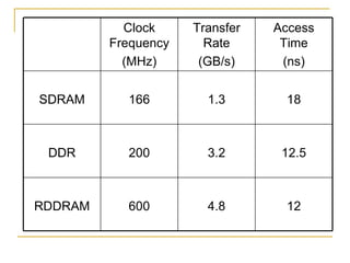
DRAM


                  Ankush Srivastava
       Email:- anksri000@gmail.com
Asynchronous DRAM
Asynchronous DRAM(ADRAM) chip is widely
used by following reason:
•Its internal architecture

•Its interface to the processor’s memory bus.
   In ADRAM, the processor gives addresses
    and control levels to the memory, indicating
    that the set of data at particular location
    should be either read from or written into the
    DRAM.
   After the access time, ADRAM either writes
    or reads the data.
   During the access time, the ADRAM performs
    the various internal functions, such as
    activating the high capacitance of the row
    and column lines, sensing data and routing
    the data out through the output buffer.
   The processor must simply wait through this
    delay, as the result the processing speed of
    the whole system is degraded.
   But the problem with ADRAM that it is need
    to insert one or more levels of SRAM cache
    between the ADRAM main memory and the
    processor.
   And SRAM is much costly compare to
    DRAM.
   In recent year, a number of changes in
    ADRAM architecture have been explored,
    and some of these now in the market. These
    are follows:
   SDRAM
   DDR DRAM
   RDRAM
Synchronous DRAM

   One of the most widely used form of DRAM is
    the synchronous DRAM(SDRAM).
   The SDRAM exchange data with the
    processor synchronized through an external
    clock signal and running at the full speed of
    the processor without any wait state.
   In SDRAM, the data moves in and out under
    control of the system clock.
   The processor issue the instruction and
    address information to SDRAM. The SDRAM
    then responds after a set of number of clock
    cycle. Meanwhile, the processor can safely
    do other tasks while the SDRAM is
    processing the request.
   As the result the processing speed of the
    whole system is increase.
Rambus DRAM
   RDRAM, developed by Rambus, has been
    adopted by Intel for its Pentium processor.
   It has become the main competitor to
    SDRAM.
   RDRAM chips are vertical packages with all
    pins one side. The chip exchanges data with
    the processor over 28 wires no more than 12
    cm long.
   The bus can address up to 320 RDRAM
    chips and is rated at 1.6 GBps.
DDR DRAM

   SDRAM is limited by the fact that it can only
    send data to the processor once per bus
    clock cycle.
   A new version of SDRAM, referred to as
    double data rate SDRAM can send data twice
    per clock cycle.
   Once on the rising edge of the clock pulse
    and once on the falling edge.
Cache DRAM

   Cache DRAM(CDRAM) integrates a small
    SRAM cache(16 kb) on to a generic DRAM
    chip.
   The SRAM on the CDRAM used in two ways:
   It can used as a true cache, consisting of 64-
    bit line.
   Used as a buffer to support the serial access
    of a block of data.
Clock     Transfer   Access
         Frequency     Rate      Time
           (MHz)      (GB/s)     (ns)


SDRAM      166         1.3       18


 DDR       200         3.2       12.5


RDDRAM     600         4.8       12

Dynamic RAM

  • 1.
    DRAM Ankush Srivastava Email:- anksri000@gmail.com
  • 2.
    Asynchronous DRAM Asynchronous DRAM(ADRAM)chip is widely used by following reason: •Its internal architecture •Its interface to the processor’s memory bus.
  • 3.
    In ADRAM, the processor gives addresses and control levels to the memory, indicating that the set of data at particular location should be either read from or written into the DRAM.  After the access time, ADRAM either writes or reads the data.
  • 4.
    During the access time, the ADRAM performs the various internal functions, such as activating the high capacitance of the row and column lines, sensing data and routing the data out through the output buffer.  The processor must simply wait through this delay, as the result the processing speed of the whole system is degraded.
  • 5.
    But the problem with ADRAM that it is need to insert one or more levels of SRAM cache between the ADRAM main memory and the processor.  And SRAM is much costly compare to DRAM.
  • 6.
    In recent year, a number of changes in ADRAM architecture have been explored, and some of these now in the market. These are follows:  SDRAM  DDR DRAM  RDRAM
  • 7.
    Synchronous DRAM  One of the most widely used form of DRAM is the synchronous DRAM(SDRAM).  The SDRAM exchange data with the processor synchronized through an external clock signal and running at the full speed of the processor without any wait state.  In SDRAM, the data moves in and out under control of the system clock.
  • 8.
    The processor issue the instruction and address information to SDRAM. The SDRAM then responds after a set of number of clock cycle. Meanwhile, the processor can safely do other tasks while the SDRAM is processing the request.  As the result the processing speed of the whole system is increase.
  • 9.
    Rambus DRAM  RDRAM, developed by Rambus, has been adopted by Intel for its Pentium processor.  It has become the main competitor to SDRAM.  RDRAM chips are vertical packages with all pins one side. The chip exchanges data with the processor over 28 wires no more than 12 cm long.  The bus can address up to 320 RDRAM chips and is rated at 1.6 GBps.
  • 10.
    DDR DRAM  SDRAM is limited by the fact that it can only send data to the processor once per bus clock cycle.  A new version of SDRAM, referred to as double data rate SDRAM can send data twice per clock cycle.  Once on the rising edge of the clock pulse and once on the falling edge.
  • 11.
    Cache DRAM  Cache DRAM(CDRAM) integrates a small SRAM cache(16 kb) on to a generic DRAM chip.  The SRAM on the CDRAM used in two ways:  It can used as a true cache, consisting of 64- bit line.  Used as a buffer to support the serial access of a block of data.
  • 12.
    Clock Transfer Access Frequency Rate Time (MHz) (GB/s) (ns) SDRAM 166 1.3 18 DDR 200 3.2 12.5 RDDRAM 600 4.8 12