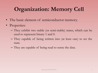
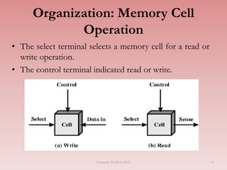
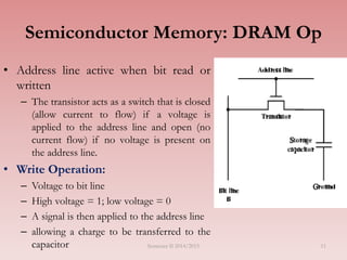
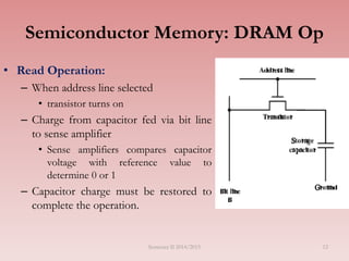
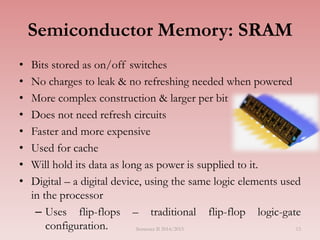
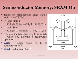
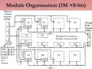
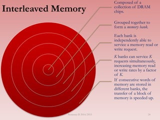
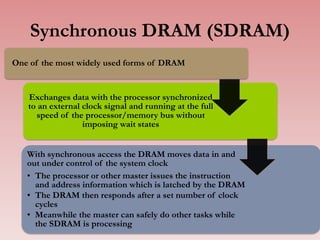
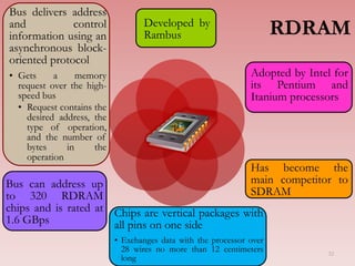
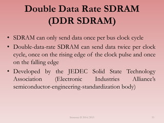
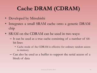
SlideShare a Scribd company logo
Madam Raini Hassan
Office: C5 - 23, Level 5, KICT Building
Department: Computer Science
Emails: hrai@iium.edu.my, hraini.iii@gmail.com
1
Du’a for Study
Semester II 2014/2015 2
LECTURE 06
Internal Memory
(Chapter 5)
Outline
• Semiconductor Main
Memory
Organization
DRAM and SRAM
Types of ROM
Chip Logic
Chip Packaging
Module Organization
Interleaved Memory
• Error Correction
• Advanced DRAM
Organization
Synchronous DRAM
Rambus DRAM
DDR SDRAM
Cache DRAM
Semester II 2014/2015 4
5
Organization: Memory Cell
• The basic element of semiconductor memory.
• Properties:
– They exhibit two stable (or semi-stable) states, which can be
used to represent binary 1 and 0.
– They capable of being written into (at least one) to set the
state.
– They are capable of being read to sense the data.
Semester II 2014/2015
6
Organization: Memory Cell
Operation
• The select terminal selects a memory cell for a read or
write operation.
• The control terminal indicated read or write.
Semester II 2014/2015
Semiconductor Memory Types
Table 5.1 Semiconductor Memory Types
The most common is referred to as Random-access Memory (RAM).
7
8
Semiconductor Memory: RAM
• Misnamed as all semiconductor memory is random
access.
• Possible for both Read/Write operation
• Volatile – once the power supply is interrupted, the data
will be lost
• Used for temporary storage
• Has 2 types:
– Dynamic
– Static
Semester II 2014/2015
9
Semiconductor Memory: DRAM
• Constructed by an array of cells, each cell containing 1
transistor and a tiny capacitor.
• These cells store data as charge in capacitors - presence or
absence of charge in a capacitor is interpreted as a binary 1
or 0
• Charges leak; the term dynamic refers to the tendency of
stored charge to leak away even with power continuously
applied.
• Requires periodic charge refreshing to maintain data storage
• The term dynamic refers to tendency of the stored charge to
leak away, even with power continuously applied
• Simpler construction Semester II 2014/2015
10
Semiconductor Memory: DRAM
• Smaller per bit
• Less expensive
• Need refresh circuits
• Slower
• Used for main memory
• Essentially analogue
– The capacitor can store any charge value within a range; level
of charge determines value
Semester II 2014/2015
11
Semiconductor Memory: DRAM Op
• Address line active when bit read or
written
– The transistor acts as a switch that is closed
(allow current to flow) if a voltage is
applied to the address line and open (no
current flow) if no voltage is present on
the address line.
• Write Operation:
– Voltage to bit line
– High voltage = 1; low voltage = 0
– A signal is then applied to the address line
– allowing a charge to be transferred to the
capacitor Semester II 2014/2015
12
Semiconductor Memory: DRAM Op
• Read Operation:
– When address line selected
• transistor turns on
– Charge from capacitor fed via bit line
to sense amplifier
• Sense amplifiers compares capacitor
voltage with reference value to
determine 0 or 1
– Capacitor charge must be restored to
complete the operation.
Semester II 2014/2015
13
Semiconductor Memory: SRAM
• Bits stored as on/off switches
• No charges to leak & no refreshing needed when powered
• More complex construction & larger per bit
• Does not need refresh circuits
• Faster and more expensive
• Used for cache
• Will hold its data as long as power is supplied to it.
• Digital – a digital device, using the same logic elements used
in the processor
– Uses flip-flops – traditional flip-flop logic-gate
configuration. Semester II 2014/2015
14
Semiconductor Memory: SRAM Op
• Transistor arrangement gives stable
logic state (T1..T4)
• In logic State 1
– C1 high, C2 low and T1 T4 off, T2 T3 on
• In logic State 0
– C2 high, C1 low andT2 T3 off, T1 T4 on
• Address line transistors T5 T6 is switch
– when on, allowing a read/write
operation
• Write – apply value to B &
compliment to B
• Read – value is on line B
Semester II 2014/2015
SRAM versus DRAM
• Both volatile
 Power must be continuously supplied to the memory to preserve the bit
values
• Dynamic cell
 Simpler to build, smaller
 More dense (smaller cells = more cells per unit area)
 Less expensive
 Requires the supporting refresh circuitry
 Tend to be favored for large memory requirements
 Used for main memory
• Static
 Faster
 Used for cache memory (both on and off chip)
Semester II 2014/2015 15
Semiconductor Memory: ROM
• Contains a permanent pattern of data that cannot be
changed or added to
• No power source is required to maintain the bit values in
memory
• Data or program is permanently in main memory and
never needs to be loaded from a secondary storage device
• Data is actually wired into the chip as part of the
fabrication process
– Disadvantages of this:
• No room for error, if one bit is wrong the whole batch of
ROMs must be thrown out
• Data insertion step includes a relatively large fixed cost
Semester II 2014/2015 16
Semiconductor Memory: Types of
ROM - PROM
• Stands for Programmable ROM
• Less expensive alternative
• Nonvolatile and may be written into only once
• Writing process is performed electrically and may be
performed by supplier or customer at a time later than
the original chip fabrication
• Special equipment is required for the writing process
• Provides flexibility and convenience
• Attractive for high volume production runs
Semester II 2014/2015 17
Semiconductor Memory: Types of
ROM -Read-Mostly Memory
EPROM
Erasable programmable read-
only memory
Erasure process can be
performed repeatedly
More expensive than PROM
but it has the advantage of
the multiple update capability
EEPROM
Electrically erasable
programmable read-only
memory
Can be written into at any
time without erasing prior
contents
Combines the advantage of
non-volatility with the
flexibility of being updatable
in place
More expensive than EPROM
Flash
Memory
Intermediate between
EPROM and EEPROM in
both cost and functionality
Uses an electrical erasing
technology, does not provide
byte-level erasure
Microchip is organized so
that a section of memory
cells are erased in a single
action or “flash”
18
• A 16Mbit chip can be organized as 1M of 16 bit words
• A bit per chip system has 16 lots of 1Mbit chip with bit 1 of
each word in chip 1 and so on
• A 16Mbit chip can be organized as a 2048 x 2048 x 4 bit
array
– Reduces number of address pins
– Multiplex row address and column address
– 11 pins to address (211=2048)
– Adding one more pin doubles range of values so x4 capacity
Chip Logic
Semester II 2014/2015 19
Chip Logic:
Typical 16 Mb DRAM (4M x 4)
20
Chip Packaging
Semester II 2014/2015 21
ModuleOrganization
Memory address
register (MAR)
256K, 8-bit word
8 pieces of
256K ×1-bit chip
22
Module Organisation (1M ×8-bit)
23
Interleaved Memory
Composed of a
collection of DRAM
chips.
Grouped together to
form a memory bank.
Each bank is
independently able to
service a memory read or
write request.
K banks can service K
requests simultaneously,
increasing memory read
or write rates by a factor
of K.
If consecutive words of
memory are stored in
different banks, the
transfer of a block of
memory is speeded up.
Semester II 2014/2015 24
25
Error Correction
• A semiconductor memory is subject to errors. 2
categories:
• Hard Failure
– Permanent physical defect so that the memory cell/cells
affected cannot reliably store data but become stuck at 0 or 1
or switch erratically between 0 and 1.
• Soft Error
– Random, non-destructive events that alters the contents of
one or memory cells.
– No permanent damage to memory.
– Can be caused by power supply problem.
Semester II 2014/2015
Semester II 2014/2015 26
Error Correction
• Both are not desirable, and most modern main memory
have systems include logic for both detecting and
correcting errors.
• The simplest of the error-correcting codes is the
Hamming code.
27
Error Correction: Error-
Correcting Code Function
1. When data are to be read into
memory, a calculation depicted as
a function f is performed on the
data to produce a code.
2. Both the code and the data are
stores, thus if an M-bit word of
data is to be stored, and the code
is of length K bits, then the actual
size of the stored word in M + K
bits.
3. When the previously stored
word is read out, the code is used
to detect and possibly correct
errors.
Semester II 2014/2015
28
Error Correction: Error-
Correcting Code Function
4. A new set of K code bits is generated
from the M data bits and compared with
the fetched bits.
5. The comparison yields one of the 3
results:
– No errors are detected. The fetched
data bits are sent out.
– An error is detected, and it is possible
to correct the error. The data bits plus
error correction bits are fed into a
corrector, which produces a corrected
set of M bits to be sent out.
– An error is detected, but it is not
possible to correct it. This condition is
reported.
6. A code is characterized by the number
of bits errors in a word that it can correct
and detect.
Semester II 2014/2015
Error
Correction:
Hamming
Error
Correcting
Code
29
Advanced DRAM Organization
• One of the most critical system bottlenecks when using high-
performance processors is the interface to main internal memory
• The traditional DRAM chip is constrained both by its internal
architecture and by its interface to the processor’s memory bus
• A number of enhancements to the basic DRAM architecture have
been explored:
Table 5.3 Performance Comparison of Some DRAM Alternatives 30
Synchronous DRAM (SDRAM)
One of the most widely used forms of DRAM
Exchanges data with the processor synchronized
to an external clock signal and running at the full
speed of the processor/memory bus without
imposing wait states
With synchronous access the DRAM moves data in and
out under control of the system clock
• The processor or other master issues the instruction
and address information which is latched by the DRAM
• The DRAM then responds after a set number of clock
cycles
• Meanwhile the master can safely do other tasks while
the SDRAM is processing 31
RDRAMDeveloped by
Rambus
Adopted by Intel for
its Pentium and
Itanium processors
Has become the
main competitor to
SDRAM
Chips are vertical packages with
all pins on one side
• Exchanges data with the processor over
28 wires no more than 12 centimeters
long
Bus can address up
to 320 RDRAM
chips and is rated at
1.6 GBps
Bus delivers address
and control
information using an
asynchronous block-
oriented protocol
• Gets a memory
request over the high-
speed bus
• Request contains the
desired address, the
type of operation,
and the number of
bytes in the
operation
32
Double Data Rate SDRAM
(DDR SDRAM)
• SDRAM can only send data once per bus clock cycle
• Double-data-rate SDRAM can send data twice per clock
cycle, once on the rising edge of the clock pulse and once
on the falling edge
• Developed by the JEDEC Solid State Technology
Association (Electronic Industries Alliance’s
semiconductor-engineering-standardization body)
Semester II 2014/2015 33
Cache DRAM (CDRAM)
• Developed by Mitsubishi
• Integrates a small SRAM cache onto a generic DRAM
chip
• SRAM on the CDRAM can be used in two ways:
– It can be used as a true cache consisting of a number of 64-
bit lines
• Cache mode of the CDRAM is effective for ordinary random access
to memory
– Can also be used as a buffer to support the serial access of a
block of data
Semester II 2014/2015 34

More Related Content

What's hot

Ch10: Virtual Memory
Ch10: Virtual MemoryCh10: Virtual Memory
Ch10: Virtual Memory
Ahmar Hashmi
 
DMA and DMA controller
DMA and DMA controllerDMA and DMA controller
DMA and DMA controller
nishant upadhyay
 
Operating system memory management
Operating system memory managementOperating system memory management
Operating system memory management
rprajat007
 
Memory Organization
Memory OrganizationMemory Organization
Memory Organization
Kamal Acharya
 
Flag registers (assembly language) with types and examples
Flag registers (assembly language) with types and examplesFlag registers (assembly language) with types and examples
Flag registers (assembly language) with types and examples
Computer_ at_home
 
Parallel processing and pipelining
Parallel processing and pipeliningParallel processing and pipelining
Parallel processing and pipelining
mahesh kumar prajapat
 
Memory organization
Memory organizationMemory organization
Memory organization
Dr. Abhineet Anand
 
8 memory management strategies
8 memory management strategies8 memory management strategies
8 memory management strategies
Dr. Loganathan R
 
Input output accessing
Input output accessingInput output accessing
Input output accessing
ankitraosingh
 
Computer organization memory hierarchy
Computer organization memory hierarchyComputer organization memory hierarchy
Computer organization memory hierarchy
AJAL A J
 
TRAFFIC LIGHT CONTROL SYSTEM USING 8085 MICROPROCESSOR
TRAFFIC LIGHT CONTROL SYSTEM USING 8085 MICROPROCESSORTRAFFIC LIGHT CONTROL SYSTEM USING 8085 MICROPROCESSOR
TRAFFIC LIGHT CONTROL SYSTEM USING 8085 MICROPROCESSOR
Subash Sambath Kumar
 
Giáo trình kỹ thuật số chương 5-6.doc
Giáo trình kỹ thuật số chương 5-6.docGiáo trình kỹ thuật số chương 5-6.doc
Giáo trình kỹ thuật số chương 5-6.doc
Man_Ebook
 
Chapter 5 a
Chapter 5 aChapter 5 a
Chapter 5 a
ececourse
 
Register organization, stack
Register organization, stackRegister organization, stack
Register organization, stack
Asif Iqbal
 
Instruction set of 8086
Instruction set of 8086Instruction set of 8086
Instruction set of 8086
aviban
 
Chapter 8 : Memory
Chapter 8 : MemoryChapter 8 : Memory
Chapter 8 : Memory
Amin Omi
 
Logical, Shift, and Rotate Instruction
Logical, Shift, and Rotate InstructionLogical, Shift, and Rotate Instruction
Logical, Shift, and Rotate Instruction
Badrul Alam
 
8051 microcontroller lecture ppt by Tarun Khaneja ( 9034406598 )
8051 microcontroller lecture ppt by Tarun Khaneja ( 9034406598 )8051 microcontroller lecture ppt by Tarun Khaneja ( 9034406598 )
8051 microcontroller lecture ppt by Tarun Khaneja ( 9034406598 )
Tarun Khaneja
 
Elements of cache design
Elements of cache designElements of cache design
Elements of cache design
Rohail Butt
 
Computer architecture instruction formats
Computer architecture instruction formatsComputer architecture instruction formats
Computer architecture instruction formats
Mazin Alwaaly
 

What's hot (20)

Ch10: Virtual Memory
Ch10: Virtual MemoryCh10: Virtual Memory
Ch10: Virtual Memory
 
DMA and DMA controller
DMA and DMA controllerDMA and DMA controller
DMA and DMA controller
 
Operating system memory management
Operating system memory managementOperating system memory management
Operating system memory management
 
Memory Organization
Memory OrganizationMemory Organization
Memory Organization
 
Flag registers (assembly language) with types and examples
Flag registers (assembly language) with types and examplesFlag registers (assembly language) with types and examples
Flag registers (assembly language) with types and examples
 
Parallel processing and pipelining
Parallel processing and pipeliningParallel processing and pipelining
Parallel processing and pipelining
 
Memory organization
Memory organizationMemory organization
Memory organization
 
8 memory management strategies
8 memory management strategies8 memory management strategies
8 memory management strategies
 
Input output accessing
Input output accessingInput output accessing
Input output accessing
 
Computer organization memory hierarchy
Computer organization memory hierarchyComputer organization memory hierarchy
Computer organization memory hierarchy
 
TRAFFIC LIGHT CONTROL SYSTEM USING 8085 MICROPROCESSOR
TRAFFIC LIGHT CONTROL SYSTEM USING 8085 MICROPROCESSORTRAFFIC LIGHT CONTROL SYSTEM USING 8085 MICROPROCESSOR
TRAFFIC LIGHT CONTROL SYSTEM USING 8085 MICROPROCESSOR
 
Giáo trình kỹ thuật số chương 5-6.doc
Giáo trình kỹ thuật số chương 5-6.docGiáo trình kỹ thuật số chương 5-6.doc
Giáo trình kỹ thuật số chương 5-6.doc
 
Chapter 5 a
Chapter 5 aChapter 5 a
Chapter 5 a
 
Register organization, stack
Register organization, stackRegister organization, stack
Register organization, stack
 
Instruction set of 8086
Instruction set of 8086Instruction set of 8086
Instruction set of 8086
 
Chapter 8 : Memory
Chapter 8 : MemoryChapter 8 : Memory
Chapter 8 : Memory
 
Logical, Shift, and Rotate Instruction
Logical, Shift, and Rotate InstructionLogical, Shift, and Rotate Instruction
Logical, Shift, and Rotate Instruction
 
8051 microcontroller lecture ppt by Tarun Khaneja ( 9034406598 )
8051 microcontroller lecture ppt by Tarun Khaneja ( 9034406598 )8051 microcontroller lecture ppt by Tarun Khaneja ( 9034406598 )
8051 microcontroller lecture ppt by Tarun Khaneja ( 9034406598 )
 
Elements of cache design
Elements of cache designElements of cache design
Elements of cache design
 
Computer architecture instruction formats
Computer architecture instruction formatsComputer architecture instruction formats
Computer architecture instruction formats
 

Viewers also liked

Internal memory
Internal memoryInternal memory
Internal memory
Siddique Ibrahim
 
Ch05 coa9e
Ch05 coa9eCh05 coa9e
Ch05 coa9e
Thodoris Skylatos
 
05 Internal Memory
05  Internal  Memory05  Internal  Memory
05 Internal Memory
Jeanie Delos Arcos
 
Internal memory
Internal memoryInternal memory
Internal memory
Federico Garcia
 
05 internal memory
05 internal memory05 internal memory
05 internal memory
Ammara Naseem
 
digital logic circuits, digital component memory unit
 digital logic circuits, digital component memory unit digital logic circuits, digital component memory unit
digital logic circuits, digital component memory unit
Rai University
 
Computer memory
Computer memoryComputer memory
Computer memory
Ambuj Rai
 
Millepede- MEMS based memory device from IBM
Millepede- MEMS based memory device from IBMMillepede- MEMS based memory device from IBM
Millepede- MEMS based memory device from IBM
Harsha
 
Internal storage of a computer system
Internal storage of a computer systemInternal storage of a computer system
Internal storage of a computer system
Palash Bhatt
 
Semiconductor memories
Semiconductor memoriesSemiconductor memories
Semiconductor memories
SambitShreeman
 
Semiconductor memory
Semiconductor memorySemiconductor memory
Semiconductor memory
Then Murugeshwari
 
Ch1-Software Engineering 9
Ch1-Software Engineering 9Ch1-Software Engineering 9
Ch1-Software Engineering 9
Ian Sommerville
 
RAM and ROM Memory Overview
RAM and ROM Memory OverviewRAM and ROM Memory Overview
RAM and ROM Memory Overview
Pankaj Khodifad
 
Lec11 Computer Architecture by Hsien-Hsin Sean Lee Georgia Tech -- Memory part3
Lec11 Computer Architecture by Hsien-Hsin Sean Lee Georgia Tech -- Memory part3Lec11 Computer Architecture by Hsien-Hsin Sean Lee Georgia Tech -- Memory part3
Lec11 Computer Architecture by Hsien-Hsin Sean Lee Georgia Tech -- Memory part3
Hsien-Hsin Sean Lee, Ph.D.
 
Semiconductor memories
Semiconductor memoriesSemiconductor memories
Semiconductor memories
kitturashmikittu
 
Internal memory
Internal memoryInternal memory
Internal memory
Robby Firmansyah
 
Basics Of Semiconductor Memories
Basics Of Semiconductor MemoriesBasics Of Semiconductor Memories
Basics Of Semiconductor Memories
Rahul Bandhe
 

Viewers also liked (17)

Internal memory
Internal memoryInternal memory
Internal memory
 
Ch05 coa9e
Ch05 coa9eCh05 coa9e
Ch05 coa9e
 
05 Internal Memory
05  Internal  Memory05  Internal  Memory
05 Internal Memory
 
Internal memory
Internal memoryInternal memory
Internal memory
 
05 internal memory
05 internal memory05 internal memory
05 internal memory
 
digital logic circuits, digital component memory unit
 digital logic circuits, digital component memory unit digital logic circuits, digital component memory unit
digital logic circuits, digital component memory unit
 
Computer memory
Computer memoryComputer memory
Computer memory
 
Millepede- MEMS based memory device from IBM
Millepede- MEMS based memory device from IBMMillepede- MEMS based memory device from IBM
Millepede- MEMS based memory device from IBM
 
Internal storage of a computer system
Internal storage of a computer systemInternal storage of a computer system
Internal storage of a computer system
 
Semiconductor memories
Semiconductor memoriesSemiconductor memories
Semiconductor memories
 
Semiconductor memory
Semiconductor memorySemiconductor memory
Semiconductor memory
 
Ch1-Software Engineering 9
Ch1-Software Engineering 9Ch1-Software Engineering 9
Ch1-Software Engineering 9
 
RAM and ROM Memory Overview
RAM and ROM Memory OverviewRAM and ROM Memory Overview
RAM and ROM Memory Overview
 
Lec11 Computer Architecture by Hsien-Hsin Sean Lee Georgia Tech -- Memory part3
Lec11 Computer Architecture by Hsien-Hsin Sean Lee Georgia Tech -- Memory part3Lec11 Computer Architecture by Hsien-Hsin Sean Lee Georgia Tech -- Memory part3
Lec11 Computer Architecture by Hsien-Hsin Sean Lee Georgia Tech -- Memory part3
 
Semiconductor memories
Semiconductor memoriesSemiconductor memories
Semiconductor memories
 
Internal memory
Internal memoryInternal memory
Internal memory
 
Basics Of Semiconductor Memories
Basics Of Semiconductor MemoriesBasics Of Semiconductor Memories
Basics Of Semiconductor Memories
 

Similar to Csc1401 lecture06 - internal memory

Memory organization
Memory organizationMemory organization
Memory organization
Dhaval Bagal
 
Computer Organisation and Architecture
Computer Organisation and ArchitectureComputer Organisation and Architecture
Computer Organisation and Architecture
Subhasis Dash
 
Computer organization memory
Computer organization memoryComputer organization memory
Computer organization memory
Deepak John
 
computer architecture and organisation
computer architecture and organisationcomputer architecture and organisation
computer architecture and organisation
RamjiChaurasiya
 
COMPUTER ARCHITECTURE-2.pptx
COMPUTER ARCHITECTURE-2.pptxCOMPUTER ARCHITECTURE-2.pptx
COMPUTER ARCHITECTURE-2.pptx
ssusere16bd9
 
Exploring Of System Hardware
Exploring Of System HardwareExploring Of System Hardware
Exploring Of System Hardware
Muhammad Nauman
 
COA (Unit_4.pptx)
COA (Unit_4.pptx)COA (Unit_4.pptx)
COA (Unit_4.pptx)
Thapar Institute
 
Unit IV Memory.pptx
Unit IV  Memory.pptxUnit IV  Memory.pptx
Unit IV Memory.pptx
madhukarvnimbalkar
 
Multiprocessor.pptx
 Multiprocessor.pptx Multiprocessor.pptx
Multiprocessor.pptx
Muhammad54342
 
Computer organisation ppt
Computer organisation pptComputer organisation ppt
Computer organisation ppt
chandkec
 
9 semiconductor memory
9 semiconductor memory9 semiconductor memory
9 semiconductor memory
Usha Mehta
 
sramanddram.ppt
sramanddram.pptsramanddram.ppt
sramanddram.ppt
AmalNath44
 
Introduction to COMPUTER’S MEMORY RAM and ROM
Introduction to COMPUTER’S MEMORY RAM and ROMIntroduction to COMPUTER’S MEMORY RAM and ROM
Introduction to COMPUTER’S MEMORY RAM and ROM
Chandrakant Divate
 
5_Embedded Systems مختصر.pdf
5_Embedded Systems  مختصر.pdf5_Embedded Systems  مختصر.pdf
5_Embedded Systems مختصر.pdf
aliamjd
 
E.s unit 4 and 5
E.s unit 4 and 5E.s unit 4 and 5
E.s unit 4 and 5
Sneha Chopra
 
MEMORY & I/O SYSTEMS
MEMORY & I/O SYSTEMS                          MEMORY & I/O SYSTEMS
MEMORY & I/O SYSTEMS
Amirthavalli Senthil
 
Bca 2nd sem-u-1.7 digital logic circuits, digital component memory unit
Bca 2nd sem-u-1.7 digital logic circuits, digital component memory unitBca 2nd sem-u-1.7 digital logic circuits, digital component memory unit
Bca 2nd sem-u-1.7 digital logic circuits, digital component memory unit
Rai University
 
Chapter5 the memory-system-jntuworld
Chapter5 the memory-system-jntuworldChapter5 the memory-system-jntuworld
Chapter5 the memory-system-jntuworld
Praveen Kumar
 
ARM architcture
ARM architcture ARM architcture
ARM architcture
Hossam Adel
 
Basic Computer Architecture
Basic Computer ArchitectureBasic Computer Architecture
Basic Computer Architecture
Yong Heui Cho
 

Similar to Csc1401 lecture06 - internal memory (20)

Memory organization
Memory organizationMemory organization
Memory organization
 
Computer Organisation and Architecture
Computer Organisation and ArchitectureComputer Organisation and Architecture
Computer Organisation and Architecture
 
Computer organization memory
Computer organization memoryComputer organization memory
Computer organization memory
 
computer architecture and organisation
computer architecture and organisationcomputer architecture and organisation
computer architecture and organisation
 
COMPUTER ARCHITECTURE-2.pptx
COMPUTER ARCHITECTURE-2.pptxCOMPUTER ARCHITECTURE-2.pptx
COMPUTER ARCHITECTURE-2.pptx
 
Exploring Of System Hardware
Exploring Of System HardwareExploring Of System Hardware
Exploring Of System Hardware
 
COA (Unit_4.pptx)
COA (Unit_4.pptx)COA (Unit_4.pptx)
COA (Unit_4.pptx)
 
Unit IV Memory.pptx
Unit IV  Memory.pptxUnit IV  Memory.pptx
Unit IV Memory.pptx
 
Multiprocessor.pptx
 Multiprocessor.pptx Multiprocessor.pptx
Multiprocessor.pptx
 
Computer organisation ppt
Computer organisation pptComputer organisation ppt
Computer organisation ppt
 
9 semiconductor memory
9 semiconductor memory9 semiconductor memory
9 semiconductor memory
 
sramanddram.ppt
sramanddram.pptsramanddram.ppt
sramanddram.ppt
 
Introduction to COMPUTER’S MEMORY RAM and ROM
Introduction to COMPUTER’S MEMORY RAM and ROMIntroduction to COMPUTER’S MEMORY RAM and ROM
Introduction to COMPUTER’S MEMORY RAM and ROM
 
5_Embedded Systems مختصر.pdf
5_Embedded Systems  مختصر.pdf5_Embedded Systems  مختصر.pdf
5_Embedded Systems مختصر.pdf
 
E.s unit 4 and 5
E.s unit 4 and 5E.s unit 4 and 5
E.s unit 4 and 5
 
MEMORY & I/O SYSTEMS
MEMORY & I/O SYSTEMS                          MEMORY & I/O SYSTEMS
MEMORY & I/O SYSTEMS
 
Bca 2nd sem-u-1.7 digital logic circuits, digital component memory unit
Bca 2nd sem-u-1.7 digital logic circuits, digital component memory unitBca 2nd sem-u-1.7 digital logic circuits, digital component memory unit
Bca 2nd sem-u-1.7 digital logic circuits, digital component memory unit
 
Chapter5 the memory-system-jntuworld
Chapter5 the memory-system-jntuworldChapter5 the memory-system-jntuworld
Chapter5 the memory-system-jntuworld
 
ARM architcture
ARM architcture ARM architcture
ARM architcture
 
Basic Computer Architecture
Basic Computer ArchitectureBasic Computer Architecture
Basic Computer Architecture
 

More from IIUM

How to use_000webhost
How to use_000webhostHow to use_000webhost
How to use_000webhost
IIUM
 
Chapter 2
Chapter 2Chapter 2
Chapter 2
IIUM
 
Chapter 1
Chapter 1Chapter 1
Chapter 1
IIUM
 
Kreydle internship-multimedia
Kreydle internship-multimediaKreydle internship-multimedia
Kreydle internship-multimedia
IIUM
 
03phpbldgblock
03phpbldgblock03phpbldgblock
03phpbldgblock
IIUM
 
Chap2 practice key
Chap2 practice keyChap2 practice key
Chap2 practice key
IIUM
 
Group p1
Group p1Group p1
Group p1
IIUM
 
Tutorial import n auto pilot blogspot friendly seo
Tutorial import n auto pilot blogspot friendly seoTutorial import n auto pilot blogspot friendly seo
Tutorial import n auto pilot blogspot friendly seo
IIUM
 
Visual sceneperception encycloperception-sage-oliva2009
Visual sceneperception encycloperception-sage-oliva2009Visual sceneperception encycloperception-sage-oliva2009
Visual sceneperception encycloperception-sage-oliva2009
IIUM
 
03 the htm_lforms
03 the htm_lforms03 the htm_lforms
03 the htm_lforms
IIUM
 
Exercise on algo analysis answer
Exercise on algo analysis   answerExercise on algo analysis   answer
Exercise on algo analysis answer
IIUM
 
Redo midterm
Redo midtermRedo midterm
Redo midterm
IIUM
 
Heaps
HeapsHeaps
Heaps
IIUM
 
Report format
Report formatReport format
Report format
IIUM
 
Edpuzzle guidelines
Edpuzzle guidelinesEdpuzzle guidelines
Edpuzzle guidelines
IIUM
 
Final Exam Paper
Final Exam PaperFinal Exam Paper
Final Exam Paper
IIUM
 
Final Exam Paper
Final Exam PaperFinal Exam Paper
Final Exam Paper
IIUM
 
Group assignment 1 s21516
Group assignment 1 s21516Group assignment 1 s21516
Group assignment 1 s21516
IIUM
 
Avl tree-rotations
Avl tree-rotationsAvl tree-rotations
Avl tree-rotations
IIUM
 
Week12 graph
Week12   graph Week12   graph
Week12 graph
IIUM
 

More from IIUM (20)

How to use_000webhost
How to use_000webhostHow to use_000webhost
How to use_000webhost
 
Chapter 2
Chapter 2Chapter 2
Chapter 2
 
Chapter 1
Chapter 1Chapter 1
Chapter 1
 
Kreydle internship-multimedia
Kreydle internship-multimediaKreydle internship-multimedia
Kreydle internship-multimedia
 
03phpbldgblock
03phpbldgblock03phpbldgblock
03phpbldgblock
 
Chap2 practice key
Chap2 practice keyChap2 practice key
Chap2 practice key
 
Group p1
Group p1Group p1
Group p1
 
Tutorial import n auto pilot blogspot friendly seo
Tutorial import n auto pilot blogspot friendly seoTutorial import n auto pilot blogspot friendly seo
Tutorial import n auto pilot blogspot friendly seo
 
Visual sceneperception encycloperception-sage-oliva2009
Visual sceneperception encycloperception-sage-oliva2009Visual sceneperception encycloperception-sage-oliva2009
Visual sceneperception encycloperception-sage-oliva2009
 
03 the htm_lforms
03 the htm_lforms03 the htm_lforms
03 the htm_lforms
 
Exercise on algo analysis answer
Exercise on algo analysis   answerExercise on algo analysis   answer
Exercise on algo analysis answer
 
Redo midterm
Redo midtermRedo midterm
Redo midterm
 
Heaps
HeapsHeaps
Heaps
 
Report format
Report formatReport format
Report format
 
Edpuzzle guidelines
Edpuzzle guidelinesEdpuzzle guidelines
Edpuzzle guidelines
 
Final Exam Paper
Final Exam PaperFinal Exam Paper
Final Exam Paper
 
Final Exam Paper
Final Exam PaperFinal Exam Paper
Final Exam Paper
 
Group assignment 1 s21516
Group assignment 1 s21516Group assignment 1 s21516
Group assignment 1 s21516
 
Avl tree-rotations
Avl tree-rotationsAvl tree-rotations
Avl tree-rotations
 
Week12 graph
Week12   graph Week12   graph
Week12 graph
 

Recently uploaded

The basics of sentences session 6pptx.pptx
The basics of sentences session 6pptx.pptxThe basics of sentences session 6pptx.pptx
The basics of sentences session 6pptx.pptx
heathfieldcps1
 
South African Journal of Science: Writing with integrity workshop (2024)
South African Journal of Science: Writing with integrity workshop (2024)South African Journal of Science: Writing with integrity workshop (2024)
South African Journal of Science: Writing with integrity workshop (2024)
Academy of Science of South Africa
 
Hindi varnamala | hindi alphabet PPT.pdf
Hindi varnamala | hindi alphabet PPT.pdfHindi varnamala | hindi alphabet PPT.pdf
Hindi varnamala | hindi alphabet PPT.pdf
Dr. Mulla Adam Ali
 
Exploiting Artificial Intelligence for Empowering Researchers and Faculty, In...
Exploiting Artificial Intelligence for Empowering Researchers and Faculty, In...Exploiting Artificial Intelligence for Empowering Researchers and Faculty, In...
Exploiting Artificial Intelligence for Empowering Researchers and Faculty, In...
Dr. Vinod Kumar Kanvaria
 
A Independência da América Espanhola LAPBOOK.pdf
A Independência da América Espanhola LAPBOOK.pdfA Independência da América Espanhola LAPBOOK.pdf
A Independência da América Espanhola LAPBOOK.pdf
Jean Carlos Nunes Paixão
 
Digital Artefact 1 - Tiny Home Environmental Design
Digital Artefact 1 - Tiny Home Environmental DesignDigital Artefact 1 - Tiny Home Environmental Design
Digital Artefact 1 - Tiny Home Environmental Design
amberjdewit93
 
C1 Rubenstein AP HuG xxxxxxxxxxxxxx.pptx
C1 Rubenstein AP HuG xxxxxxxxxxxxxx.pptxC1 Rubenstein AP HuG xxxxxxxxxxxxxx.pptx
C1 Rubenstein AP HuG xxxxxxxxxxxxxx.pptx
mulvey2
 
Assessment and Planning in Educational technology.pptx
Assessment and Planning in Educational technology.pptxAssessment and Planning in Educational technology.pptx
Assessment and Planning in Educational technology.pptx
Kavitha Krishnan
 
Lapbook sobre os Regimes Totalitários.pdf
Lapbook sobre os Regimes Totalitários.pdfLapbook sobre os Regimes Totalitários.pdf
Lapbook sobre os Regimes Totalitários.pdf
Jean Carlos Nunes Paixão
 
How to Manage Your Lost Opportunities in Odoo 17 CRM
How to Manage Your Lost Opportunities in Odoo 17 CRMHow to Manage Your Lost Opportunities in Odoo 17 CRM
How to Manage Your Lost Opportunities in Odoo 17 CRM
Celine George
 
The simplified electron and muon model, Oscillating Spacetime: The Foundation...
The simplified electron and muon model, Oscillating Spacetime: The Foundation...The simplified electron and muon model, Oscillating Spacetime: The Foundation...
The simplified electron and muon model, Oscillating Spacetime: The Foundation...
RitikBhardwaj56
 
Film vocab for eal 3 students: Australia the movie
Film vocab for eal 3 students: Australia the movieFilm vocab for eal 3 students: Australia the movie
Film vocab for eal 3 students: Australia the movie
Nicholas Montgomery
 
PCOS corelations and management through Ayurveda.
PCOS corelations and management through Ayurveda.PCOS corelations and management through Ayurveda.
PCOS corelations and management through Ayurveda.
Dr. Shivangi Singh Parihar
 
BÀI TẬP BỔ TRỢ TIẾNG ANH 8 CẢ NĂM - GLOBAL SUCCESS - NĂM HỌC 2023-2024 (CÓ FI...
BÀI TẬP BỔ TRỢ TIẾNG ANH 8 CẢ NĂM - GLOBAL SUCCESS - NĂM HỌC 2023-2024 (CÓ FI...BÀI TẬP BỔ TRỢ TIẾNG ANH 8 CẢ NĂM - GLOBAL SUCCESS - NĂM HỌC 2023-2024 (CÓ FI...
BÀI TẬP BỔ TRỢ TIẾNG ANH 8 CẢ NĂM - GLOBAL SUCCESS - NĂM HỌC 2023-2024 (CÓ FI...
Nguyen Thanh Tu Collection
 
Top five deadliest dog breeds in America
Top five deadliest dog breeds in AmericaTop five deadliest dog breeds in America
Top five deadliest dog breeds in America
Bisnar Chase Personal Injury Attorneys
 
The History of Stoke Newington Street Names
The History of Stoke Newington Street NamesThe History of Stoke Newington Street Names
The History of Stoke Newington Street Names
History of Stoke Newington
 
Main Java[All of the Base Concepts}.docx
Main Java[All of the Base Concepts}.docxMain Java[All of the Base Concepts}.docx
Main Java[All of the Base Concepts}.docx
adhitya5119
 
CACJapan - GROUP Presentation 1- Wk 4.pdf
CACJapan - GROUP Presentation 1- Wk 4.pdfCACJapan - GROUP Presentation 1- Wk 4.pdf
CACJapan - GROUP Presentation 1- Wk 4.pdf
camakaiclarkmusic
 
Natural birth techniques - Mrs.Akanksha Trivedi Rama University
Natural birth techniques - Mrs.Akanksha Trivedi Rama UniversityNatural birth techniques - Mrs.Akanksha Trivedi Rama University
Natural birth techniques - Mrs.Akanksha Trivedi Rama University
Akanksha trivedi rama nursing college kanpur.
 
RPMS TEMPLATE FOR SCHOOL YEAR 2023-2024 FOR TEACHER 1 TO TEACHER 3
RPMS TEMPLATE FOR SCHOOL YEAR 2023-2024 FOR TEACHER 1 TO TEACHER 3RPMS TEMPLATE FOR SCHOOL YEAR 2023-2024 FOR TEACHER 1 TO TEACHER 3
RPMS TEMPLATE FOR SCHOOL YEAR 2023-2024 FOR TEACHER 1 TO TEACHER 3
IreneSebastianRueco1
 

Recently uploaded (20)

The basics of sentences session 6pptx.pptx
The basics of sentences session 6pptx.pptxThe basics of sentences session 6pptx.pptx
The basics of sentences session 6pptx.pptx
 
South African Journal of Science: Writing with integrity workshop (2024)
South African Journal of Science: Writing with integrity workshop (2024)South African Journal of Science: Writing with integrity workshop (2024)
South African Journal of Science: Writing with integrity workshop (2024)
 
Hindi varnamala | hindi alphabet PPT.pdf
Hindi varnamala | hindi alphabet PPT.pdfHindi varnamala | hindi alphabet PPT.pdf
Hindi varnamala | hindi alphabet PPT.pdf
 
Exploiting Artificial Intelligence for Empowering Researchers and Faculty, In...
Exploiting Artificial Intelligence for Empowering Researchers and Faculty, In...Exploiting Artificial Intelligence for Empowering Researchers and Faculty, In...
Exploiting Artificial Intelligence for Empowering Researchers and Faculty, In...
 
A Independência da América Espanhola LAPBOOK.pdf
A Independência da América Espanhola LAPBOOK.pdfA Independência da América Espanhola LAPBOOK.pdf
A Independência da América Espanhola LAPBOOK.pdf
 
Digital Artefact 1 - Tiny Home Environmental Design
Digital Artefact 1 - Tiny Home Environmental DesignDigital Artefact 1 - Tiny Home Environmental Design
Digital Artefact 1 - Tiny Home Environmental Design
 
C1 Rubenstein AP HuG xxxxxxxxxxxxxx.pptx
C1 Rubenstein AP HuG xxxxxxxxxxxxxx.pptxC1 Rubenstein AP HuG xxxxxxxxxxxxxx.pptx
C1 Rubenstein AP HuG xxxxxxxxxxxxxx.pptx
 
Assessment and Planning in Educational technology.pptx
Assessment and Planning in Educational technology.pptxAssessment and Planning in Educational technology.pptx
Assessment and Planning in Educational technology.pptx
 
Lapbook sobre os Regimes Totalitários.pdf
Lapbook sobre os Regimes Totalitários.pdfLapbook sobre os Regimes Totalitários.pdf
Lapbook sobre os Regimes Totalitários.pdf
 
How to Manage Your Lost Opportunities in Odoo 17 CRM
How to Manage Your Lost Opportunities in Odoo 17 CRMHow to Manage Your Lost Opportunities in Odoo 17 CRM
How to Manage Your Lost Opportunities in Odoo 17 CRM
 
The simplified electron and muon model, Oscillating Spacetime: The Foundation...
The simplified electron and muon model, Oscillating Spacetime: The Foundation...The simplified electron and muon model, Oscillating Spacetime: The Foundation...
The simplified electron and muon model, Oscillating Spacetime: The Foundation...
 
Film vocab for eal 3 students: Australia the movie
Film vocab for eal 3 students: Australia the movieFilm vocab for eal 3 students: Australia the movie
Film vocab for eal 3 students: Australia the movie
 
PCOS corelations and management through Ayurveda.
PCOS corelations and management through Ayurveda.PCOS corelations and management through Ayurveda.
PCOS corelations and management through Ayurveda.
 
BÀI TẬP BỔ TRỢ TIẾNG ANH 8 CẢ NĂM - GLOBAL SUCCESS - NĂM HỌC 2023-2024 (CÓ FI...
BÀI TẬP BỔ TRỢ TIẾNG ANH 8 CẢ NĂM - GLOBAL SUCCESS - NĂM HỌC 2023-2024 (CÓ FI...BÀI TẬP BỔ TRỢ TIẾNG ANH 8 CẢ NĂM - GLOBAL SUCCESS - NĂM HỌC 2023-2024 (CÓ FI...
BÀI TẬP BỔ TRỢ TIẾNG ANH 8 CẢ NĂM - GLOBAL SUCCESS - NĂM HỌC 2023-2024 (CÓ FI...
 
Top five deadliest dog breeds in America
Top five deadliest dog breeds in AmericaTop five deadliest dog breeds in America
Top five deadliest dog breeds in America
 
The History of Stoke Newington Street Names
The History of Stoke Newington Street NamesThe History of Stoke Newington Street Names
The History of Stoke Newington Street Names
 
Main Java[All of the Base Concepts}.docx
Main Java[All of the Base Concepts}.docxMain Java[All of the Base Concepts}.docx
Main Java[All of the Base Concepts}.docx
 
CACJapan - GROUP Presentation 1- Wk 4.pdf
CACJapan - GROUP Presentation 1- Wk 4.pdfCACJapan - GROUP Presentation 1- Wk 4.pdf
CACJapan - GROUP Presentation 1- Wk 4.pdf
 
Natural birth techniques - Mrs.Akanksha Trivedi Rama University
Natural birth techniques - Mrs.Akanksha Trivedi Rama UniversityNatural birth techniques - Mrs.Akanksha Trivedi Rama University
Natural birth techniques - Mrs.Akanksha Trivedi Rama University
 
RPMS TEMPLATE FOR SCHOOL YEAR 2023-2024 FOR TEACHER 1 TO TEACHER 3
RPMS TEMPLATE FOR SCHOOL YEAR 2023-2024 FOR TEACHER 1 TO TEACHER 3RPMS TEMPLATE FOR SCHOOL YEAR 2023-2024 FOR TEACHER 1 TO TEACHER 3
RPMS TEMPLATE FOR SCHOOL YEAR 2023-2024 FOR TEACHER 1 TO TEACHER 3
 

Csc1401 lecture06 - internal memory

  • 1. Madam Raini Hassan Office: C5 - 23, Level 5, KICT Building Department: Computer Science Emails: hrai@iium.edu.my, hraini.iii@gmail.com 1
  • 2. Du’a for Study Semester II 2014/2015 2
  • 4. Outline • Semiconductor Main Memory Organization DRAM and SRAM Types of ROM Chip Logic Chip Packaging Module Organization Interleaved Memory • Error Correction • Advanced DRAM Organization Synchronous DRAM Rambus DRAM DDR SDRAM Cache DRAM Semester II 2014/2015 4
  • 5. 5 Organization: Memory Cell • The basic element of semiconductor memory. • Properties: – They exhibit two stable (or semi-stable) states, which can be used to represent binary 1 and 0. – They capable of being written into (at least one) to set the state. – They are capable of being read to sense the data. Semester II 2014/2015
  • 6. 6 Organization: Memory Cell Operation • The select terminal selects a memory cell for a read or write operation. • The control terminal indicated read or write. Semester II 2014/2015
  • 7. Semiconductor Memory Types Table 5.1 Semiconductor Memory Types The most common is referred to as Random-access Memory (RAM). 7
  • 8. 8 Semiconductor Memory: RAM • Misnamed as all semiconductor memory is random access. • Possible for both Read/Write operation • Volatile – once the power supply is interrupted, the data will be lost • Used for temporary storage • Has 2 types: – Dynamic – Static Semester II 2014/2015
  • 9. 9 Semiconductor Memory: DRAM • Constructed by an array of cells, each cell containing 1 transistor and a tiny capacitor. • These cells store data as charge in capacitors - presence or absence of charge in a capacitor is interpreted as a binary 1 or 0 • Charges leak; the term dynamic refers to the tendency of stored charge to leak away even with power continuously applied. • Requires periodic charge refreshing to maintain data storage • The term dynamic refers to tendency of the stored charge to leak away, even with power continuously applied • Simpler construction Semester II 2014/2015
  • 10. 10 Semiconductor Memory: DRAM • Smaller per bit • Less expensive • Need refresh circuits • Slower • Used for main memory • Essentially analogue – The capacitor can store any charge value within a range; level of charge determines value Semester II 2014/2015
  • 11. 11 Semiconductor Memory: DRAM Op • Address line active when bit read or written – The transistor acts as a switch that is closed (allow current to flow) if a voltage is applied to the address line and open (no current flow) if no voltage is present on the address line. • Write Operation: – Voltage to bit line – High voltage = 1; low voltage = 0 – A signal is then applied to the address line – allowing a charge to be transferred to the capacitor Semester II 2014/2015
  • 12. 12 Semiconductor Memory: DRAM Op • Read Operation: – When address line selected • transistor turns on – Charge from capacitor fed via bit line to sense amplifier • Sense amplifiers compares capacitor voltage with reference value to determine 0 or 1 – Capacitor charge must be restored to complete the operation. Semester II 2014/2015
  • 13. 13 Semiconductor Memory: SRAM • Bits stored as on/off switches • No charges to leak & no refreshing needed when powered • More complex construction & larger per bit • Does not need refresh circuits • Faster and more expensive • Used for cache • Will hold its data as long as power is supplied to it. • Digital – a digital device, using the same logic elements used in the processor – Uses flip-flops – traditional flip-flop logic-gate configuration. Semester II 2014/2015
  • 14. 14 Semiconductor Memory: SRAM Op • Transistor arrangement gives stable logic state (T1..T4) • In logic State 1 – C1 high, C2 low and T1 T4 off, T2 T3 on • In logic State 0 – C2 high, C1 low andT2 T3 off, T1 T4 on • Address line transistors T5 T6 is switch – when on, allowing a read/write operation • Write – apply value to B & compliment to B • Read – value is on line B Semester II 2014/2015
  • 15. SRAM versus DRAM • Both volatile  Power must be continuously supplied to the memory to preserve the bit values • Dynamic cell  Simpler to build, smaller  More dense (smaller cells = more cells per unit area)  Less expensive  Requires the supporting refresh circuitry  Tend to be favored for large memory requirements  Used for main memory • Static  Faster  Used for cache memory (both on and off chip) Semester II 2014/2015 15
  • 16. Semiconductor Memory: ROM • Contains a permanent pattern of data that cannot be changed or added to • No power source is required to maintain the bit values in memory • Data or program is permanently in main memory and never needs to be loaded from a secondary storage device • Data is actually wired into the chip as part of the fabrication process – Disadvantages of this: • No room for error, if one bit is wrong the whole batch of ROMs must be thrown out • Data insertion step includes a relatively large fixed cost Semester II 2014/2015 16
  • 17. Semiconductor Memory: Types of ROM - PROM • Stands for Programmable ROM • Less expensive alternative • Nonvolatile and may be written into only once • Writing process is performed electrically and may be performed by supplier or customer at a time later than the original chip fabrication • Special equipment is required for the writing process • Provides flexibility and convenience • Attractive for high volume production runs Semester II 2014/2015 17
  • 18. Semiconductor Memory: Types of ROM -Read-Mostly Memory EPROM Erasable programmable read- only memory Erasure process can be performed repeatedly More expensive than PROM but it has the advantage of the multiple update capability EEPROM Electrically erasable programmable read-only memory Can be written into at any time without erasing prior contents Combines the advantage of non-volatility with the flexibility of being updatable in place More expensive than EPROM Flash Memory Intermediate between EPROM and EEPROM in both cost and functionality Uses an electrical erasing technology, does not provide byte-level erasure Microchip is organized so that a section of memory cells are erased in a single action or “flash” 18
  • 19. • A 16Mbit chip can be organized as 1M of 16 bit words • A bit per chip system has 16 lots of 1Mbit chip with bit 1 of each word in chip 1 and so on • A 16Mbit chip can be organized as a 2048 x 2048 x 4 bit array – Reduces number of address pins – Multiplex row address and column address – 11 pins to address (211=2048) – Adding one more pin doubles range of values so x4 capacity Chip Logic Semester II 2014/2015 19
  • 20. Chip Logic: Typical 16 Mb DRAM (4M x 4) 20
  • 22. ModuleOrganization Memory address register (MAR) 256K, 8-bit word 8 pieces of 256K ×1-bit chip 22
  • 23. Module Organisation (1M ×8-bit) 23
  • 24. Interleaved Memory Composed of a collection of DRAM chips. Grouped together to form a memory bank. Each bank is independently able to service a memory read or write request. K banks can service K requests simultaneously, increasing memory read or write rates by a factor of K. If consecutive words of memory are stored in different banks, the transfer of a block of memory is speeded up. Semester II 2014/2015 24
  • 25. 25 Error Correction • A semiconductor memory is subject to errors. 2 categories: • Hard Failure – Permanent physical defect so that the memory cell/cells affected cannot reliably store data but become stuck at 0 or 1 or switch erratically between 0 and 1. • Soft Error – Random, non-destructive events that alters the contents of one or memory cells. – No permanent damage to memory. – Can be caused by power supply problem. Semester II 2014/2015
  • 26. Semester II 2014/2015 26 Error Correction • Both are not desirable, and most modern main memory have systems include logic for both detecting and correcting errors. • The simplest of the error-correcting codes is the Hamming code.
  • 27. 27 Error Correction: Error- Correcting Code Function 1. When data are to be read into memory, a calculation depicted as a function f is performed on the data to produce a code. 2. Both the code and the data are stores, thus if an M-bit word of data is to be stored, and the code is of length K bits, then the actual size of the stored word in M + K bits. 3. When the previously stored word is read out, the code is used to detect and possibly correct errors. Semester II 2014/2015
  • 28. 28 Error Correction: Error- Correcting Code Function 4. A new set of K code bits is generated from the M data bits and compared with the fetched bits. 5. The comparison yields one of the 3 results: – No errors are detected. The fetched data bits are sent out. – An error is detected, and it is possible to correct the error. The data bits plus error correction bits are fed into a corrector, which produces a corrected set of M bits to be sent out. – An error is detected, but it is not possible to correct it. This condition is reported. 6. A code is characterized by the number of bits errors in a word that it can correct and detect. Semester II 2014/2015
  • 30. Advanced DRAM Organization • One of the most critical system bottlenecks when using high- performance processors is the interface to main internal memory • The traditional DRAM chip is constrained both by its internal architecture and by its interface to the processor’s memory bus • A number of enhancements to the basic DRAM architecture have been explored: Table 5.3 Performance Comparison of Some DRAM Alternatives 30
  • 31. Synchronous DRAM (SDRAM) One of the most widely used forms of DRAM Exchanges data with the processor synchronized to an external clock signal and running at the full speed of the processor/memory bus without imposing wait states With synchronous access the DRAM moves data in and out under control of the system clock • The processor or other master issues the instruction and address information which is latched by the DRAM • The DRAM then responds after a set number of clock cycles • Meanwhile the master can safely do other tasks while the SDRAM is processing 31
  • 32. RDRAMDeveloped by Rambus Adopted by Intel for its Pentium and Itanium processors Has become the main competitor to SDRAM Chips are vertical packages with all pins on one side • Exchanges data with the processor over 28 wires no more than 12 centimeters long Bus can address up to 320 RDRAM chips and is rated at 1.6 GBps Bus delivers address and control information using an asynchronous block- oriented protocol • Gets a memory request over the high- speed bus • Request contains the desired address, the type of operation, and the number of bytes in the operation 32
  • 33. Double Data Rate SDRAM (DDR SDRAM) • SDRAM can only send data once per bus clock cycle • Double-data-rate SDRAM can send data twice per clock cycle, once on the rising edge of the clock pulse and once on the falling edge • Developed by the JEDEC Solid State Technology Association (Electronic Industries Alliance’s semiconductor-engineering-standardization body) Semester II 2014/2015 33
  • 34. Cache DRAM (CDRAM) • Developed by Mitsubishi • Integrates a small SRAM cache onto a generic DRAM chip • SRAM on the CDRAM can be used in two ways: – It can be used as a true cache consisting of a number of 64- bit lines • Cache mode of the CDRAM is effective for ordinary random access to memory – Can also be used as a buffer to support the serial access of a block of data Semester II 2014/2015 34