Downloaded 1,752 times
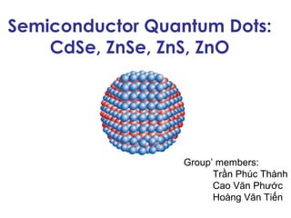

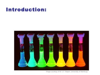


E = g lk+ 2 + − − + r m 0 m 0 4 ε 0 h ( ε 0 2 e 0 m 0 8 em hm πεr 2 2ε ) m m hm Brus, L. E. J. Phys. Chem. 1986, 90, 2555 Semiconductor quantum dots are nanocrystals made of semiconductor materials such as CdSe, ZnSe, ZnS, and ZnO. They exhibit size-dependent optical and electronic properties due to


