It's simple to understand the synthesis. Hydrothermal method is a chemical reaction in water in a sealed pressure vessel, which is in fact a type of reaction at both high temperature and pressure.
Classification of Nanostructures by Peeyush MishraPeeyush Mishra
In this presentation, I have tried to define Nanostructures and discuss various types of Nanostructures. I have also compared the ways in which Nanomaterials can be synthesized.
The following presentation is only for quick reference. I would advise you to read the theoretical aspects of the respective topic and then use this presentation for your last minute revision. I hope it helps you..!!
Mayur D. Chauhan
here you can find the most rare topics in detail
all fields of chemistry are deeply understood here for presenting the lectures
stay blessed and keep supporting
The following presentation is only for quick reference. I would advise you to read the theoretical aspects of the respective topic and then use this presentation for your last minute revision. I hope it helps you..!!
Mayur D. Chauhan
The following presentation is only for quick reference. I would advise you to read the theoretical aspects of the respective topic and then use this presentation for your last minute revision. I hope it helps you..!!
Mayur D. Chauhan
20091116-17
Curso de Genómica Aplicada a la Medicina Clínica (MADRID)
---
Las macromoléculas se comportan como diminutas máquinas para realizar sus funciones biológicas dentro de las células.
Si bien la estructura (en los diferentes niveles) viede dada por la secuencia de las proteínas, la función más que a la propia estructura la deben a las diferentes conformaciones que pueden adoptar.
Tanto la difracción de rayos X, como las técnicas de microscopía electrónica son capaces de resolver las estructuras 3D de un amplio rango de biomoleculas. Combinandolas obtenemos "modelos híbridos" que se benefician de las mejores caracteristicas de estas técnicas que se complementan.
PeppeR es una aplicación de integración de datos, que permite ver los modelos híbridos almacenados en EMDB, junto con anotaciones de otras muchas bases de datos de genomica, proteomica, etc.
Nanotechnology & its Nanowires Application (By-Saquib Khan)SAQUIB KHAN
Appropriate presentation for Nanotechnology & Nanowires Application. along with Nanowiresbattery.
By- SAQUIB KHAN
B.TECH.MECHANICAL ENGG.(First Year)
INTEGRAL UNIVERSITY
Lucknow
A presentation about nanoelectronics-what it is and why it is used widely nowadays, its advantages and industrial applications and the future use. Also describes some problems faced by nanoelectronics.
In this article, we are introducing some technique of growth Nanowire for Nanostructures for physics, A Nanowire considered as a Nanostructure which is build blocks for the generation of electrons protons neutrons positions and the sensor and also the energy applications. In this project, we are to synthesis and growth of semiconductor nanowire made by metallic both of the axial and radial structure and their properties discuss here. In one-dimensional nanostructure of control, density States turned into the electronic and optic properties. There is a new technique of growth metallic and semiconducting material develop in the International Science. A nanowire is a nanostructure, with the diameter of the order of a nanometer (10−9 meters) and an unconstrained length. At these scales, quantum mechanical effects are important — which coined the term "quantum wires.” Quantum confinement produces new material behaviour/phenomena. Based on the degree of confinement different Structures arise.
brief description on how nano technology and carbon nanotubes work in engineering...future scope of carbon nano tubes and development of existing machines with nanoparticles
Quantum dots for optoelectronic devices - phdassistancePhD Assistance
Nanometre-scale semiconductor chips have been imagined as next-generation technology with high functionality and convergence. Quantum dots, also known as artificial atoms, have special properties owing to their quantum confinement in all three dimensions. Quantum dots have a lot of interest in optoelectronic systems because of their special properties.
For decades, self-assembled nanostructures have been a topic of considerable concern and significance.
Learn More:https://bit.ly/3xJJAiZ
Contact Us:
Website: https://www.phdassistance.com/
UK: +44 7537144372
India No:+91-9176966446
Email: info@phdassistance.com
Nanotechnology and Its Applications which are related to the field of engineering and mainly bio-nanotechnology, electronics and green nanotechnology in India.
Embracing GenAI - A Strategic ImperativePeter Windle
Artificial Intelligence (AI) technologies such as Generative AI, Image Generators and Large Language Models have had a dramatic impact on teaching, learning and assessment over the past 18 months. The most immediate threat AI posed was to Academic Integrity with Higher Education Institutes (HEIs) focusing their efforts on combating the use of GenAI in assessment. Guidelines were developed for staff and students, policies put in place too. Innovative educators have forged paths in the use of Generative AI for teaching, learning and assessments leading to pockets of transformation springing up across HEIs, often with little or no top-down guidance, support or direction.
This Gasta posits a strategic approach to integrating AI into HEIs to prepare staff, students and the curriculum for an evolving world and workplace. We will highlight the advantages of working with these technologies beyond the realm of teaching, learning and assessment by considering prompt engineering skills, industry impact, curriculum changes, and the need for staff upskilling. In contrast, not engaging strategically with Generative AI poses risks, including falling behind peers, missed opportunities and failing to ensure our graduates remain employable. The rapid evolution of AI technologies necessitates a proactive and strategic approach if we are to remain relevant.
Read| The latest issue of The Challenger is here! We are thrilled to announce that our school paper has qualified for the NATIONAL SCHOOLS PRESS CONFERENCE (NSPC) 2024. Thank you for your unwavering support and trust. Dive into the stories that made us stand out!
Introduction to AI for Nonprofits with Tapp NetworkTechSoup
Dive into the world of AI! Experts Jon Hill and Tareq Monaur will guide you through AI's role in enhancing nonprofit websites and basic marketing strategies, making it easy to understand and apply.
Instructions for Submissions thorugh G- Classroom.pptxJheel Barad
This presentation provides a briefing on how to upload submissions and documents in Google Classroom. It was prepared as part of an orientation for new Sainik School in-service teacher trainees. As a training officer, my goal is to ensure that you are comfortable and proficient with this essential tool for managing assignments and fostering student engagement.
Acetabularia Information For Class 9 .docxvaibhavrinwa19
Acetabularia acetabulum is a single-celled green alga that in its vegetative state is morphologically differentiated into a basal rhizoid and an axially elongated stalk, which bears whorls of branching hairs. The single diploid nucleus resides in the rhizoid.
2024.06.01 Introducing a competency framework for languag learning materials ...Sandy Millin
http://sandymillin.wordpress.com/iateflwebinar2024
Published classroom materials form the basis of syllabuses, drive teacher professional development, and have a potentially huge influence on learners, teachers and education systems. All teachers also create their own materials, whether a few sentences on a blackboard, a highly-structured fully-realised online course, or anything in between. Despite this, the knowledge and skills needed to create effective language learning materials are rarely part of teacher training, and are mostly learnt by trial and error.
Knowledge and skills frameworks, generally called competency frameworks, for ELT teachers, trainers and managers have existed for a few years now. However, until I created one for my MA dissertation, there wasn’t one drawing together what we need to know and do to be able to effectively produce language learning materials.
This webinar will introduce you to my framework, highlighting the key competencies I identified from my research. It will also show how anybody involved in language teaching (any language, not just English!), teacher training, managing schools or developing language learning materials can benefit from using the framework.
Synthetic Fiber Construction in lab .pptxPavel ( NSTU)
Synthetic fiber production is a fascinating and complex field that blends chemistry, engineering, and environmental science. By understanding these aspects, students can gain a comprehensive view of synthetic fiber production, its impact on society and the environment, and the potential for future innovations. Synthetic fibers play a crucial role in modern society, impacting various aspects of daily life, industry, and the environment. ynthetic fibers are integral to modern life, offering a range of benefits from cost-effectiveness and versatility to innovative applications and performance characteristics. While they pose environmental challenges, ongoing research and development aim to create more sustainable and eco-friendly alternatives. Understanding the importance of synthetic fibers helps in appreciating their role in the economy, industry, and daily life, while also emphasizing the need for sustainable practices and innovation.
Francesca Gottschalk - How can education support child empowerment.pptxEduSkills OECD
Francesca Gottschalk from the OECD’s Centre for Educational Research and Innovation presents at the Ask an Expert Webinar: How can education support child empowerment?
2. INTRODUCTION
Nanoscale electronics could hold the promise of
powering future electronic devices that can
outperform existing devices and open up totally
new opportunities.
It will require conceptually new device building
blocks, scalable circuit architectures, and
fundamentally different fabrication strategies.
3. 1D nanostructures represent the smallest
dimension structure that can efficiently transport
electrical carriers
1D nanostructures can also exhibit critical device
function, and thus can be exploited as both the
wiring and device elements in future
architectures for functional nanosystems
In this regard, two material classes:
semiconductor nanowires (NWs)
carbon nanotubes (NTs)
have shown particular promise
4. NTs have been used to fabricate field effect
transistors, diodes, and logic circuits.
Problems with Nanotubes to made devices:
Difficulties to control whether building blocks are
semiconducting or metallic
Difficulties in manipulating individual NTs
So, to date, device fabrication by NT largely is a
random event, thus pose a significant barrier to
achieving highly integrated nanocircuits
5. Advantages of Nanowires
NW devices can be assembled in a rational and
predictable because:
Nanowires can be precisely controlled during
synthesis,
chemical composition,
diameter,
length,
doping/electronic properties
It is possible to combine distinct NW building
blocks in ways not possible in conventional
electronics.
NWs thus represent the best-defined class of
nanoscale building blocks, and this precise
control over key variables has correspondingly
enabled a wide range of devices and integration
strategies to be pursued
6. WHAT ARE NANOWIRES?
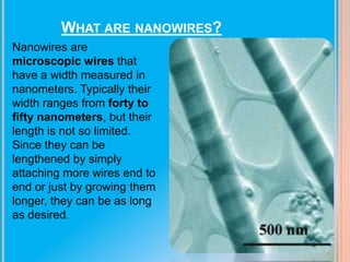
Nanowires are
microscopic wires that
have a width measured in
nanometers. Typically their
width ranges from forty to
fifty nanometers, but their
length is not so limited.
Since they can be
lengthened by simply
attaching more wires end to
end or just by growing them
longer, they can be as long
as desired.
7.
Diameter of nanowires range from a single atom
to a few hundreds of nanometers.
Length varies from a few atoms to many microns
Different name of nanowires in literature:
Whiskers, fibers: 1D structures ranging from
several nanometers to several hundred
microns
Nanowires: Wires with large
aspect ratios (e.g. >20),
Nanorods: Wires with small
aspect ratios.
NanoContacts: short wires bridged
between two larger electrodes.
8. SYNTHESIS OF NANOWIRES
Some of the recent successful synthesis of
nanowires are based on the so-called vapor-liquidsolid (VLS) mechanism
11. VAPOR LIQUID SOLID GROWTH (VLS)
TEM and selected area diffraction image of a single
crystal ZnO nanorod.(~20 nm width).
12. PROPERTIES AND APPLICATION OF
NANOWIRES
Nanowires are promising materials for many novel
applications
Not only because of their unique geometry, but
also because they possess many
unique physical properties, including :
electrical
magnetic
optical
mechanical
13. MAGNETIC PROPERTIES
•
Actually the magnetic properties of nanowires depend
on the wire diameter and aspect ratio
•
It is possible to control the magnetic properties of the
nanowires by controlling the fabrication parameters
•
Remanence ratio, which measures the remanence
magnetization after switching off the external magnetic
field
•
Coercivity, which is the coercive field required to
demagnetize the magnet after full magnetization.
•
Giant Magnetoresistance (GMR)
14. OPTICAL
PROPERTIES
•
Controlling the flow of optically encoded
information with nanometer-scale accuracy over
distances of many microns, which may find
applications in future high-density optical
computing.
•
Silicon nanowires coated with SiC show stable
photoluminescence at room temperature
15. STRIPED NANOWIRES
Striped nanowires are capable of performing more
than one task along the same wire.
They
are striped with
different
materials that
posses different
properties,
an attribute which
allows different
operations to be performed at
the
same time. This also enables
devices to be more compacted because fewer
wires are needed; each nanowire is serving multiple
functions
16. WHY ARE NANOWIRES NOT BEING
IMPLEMENTED?
Nanowires are not being heavily manufactured because they are
still in the development stage and are only produced in the
laboratory. Until production has been streamlined,
made easier and faster, they will not be heavily
manufactured for commercial purposes.
Furthermore, though they are 4 or 5 times more
effective than current technology, an industry-wide
technology overhaul is not cost effective at the moment
17. WHAT USES ARE NANOWIRES BEING
DEVELOPED FOR?
IBM has been doing research on forming U-shaped
nanowires to create a “racetrack memory”. This
method would allow IBM to create a memory
system with no moving parts and far greater
storage than flash memory. This U-shape is formed
with closely arranged nanowires, allowing fast
transmissions and increasing storage size without
adding to the overall size of the device.
Nanowires are also being developed for prototype
sensors. These sensors will be used on gases and
biological molecules
18. WHAT GOOD ARE NANOWIRES?
Some uses of nanowires include:
Data storage/transfer
Batteries/generators
Transistors
LED’s
Optoelectronic devices
Biochemical sensors
Heat-pumping Thermoelectric devices
21. CONCLUSION
•
•
•
•
•
•
Challenges:
The insufficient control of the properties of individual
building blocks
Low device-to-device reproducibility
Lack of reliable methods for assembling and
integrating building blocks into circuits
Advances:
Synthesis of nanoscale building blocks with precisely
controlled chemical composition, physical
dimension, and electronic, optical properties
Some strategies for the assembly of building blocks
into increasingly complex structures
New nanodevice concepts that can be implemented in
high yield by assembly approaches
22. REFERENCE
Essentials of nanotechnology; Jeremy ramsdan
Nanotubes& Nanowires; C N Ram Rao
Nanotubes& Nanowires; Peter John Burke
Wikipedia
Nanowires: A Platform for Nanoscience&
Nanotechnology; Charles M. Lieber