Quantum Dots
•Download as PPTX, PDF•
2 likes•1,011 views

properties, synthesis and applications of quantum dots

Recommended
More Related Content
What's hot
What's hot (20)
Similar to Quantum Dots
Similar to Quantum Dots (20)
Recently uploaded
Recently uploaded (20)
Quantum Dots
- 2. What really Quantum Dots are?
- 3. QUANTUM DOTS (QDs) are nanometer- scale semiconductor crystals composed of groups II-VI (e.g.- CdS, CdSe ) or III-V elements. They are defined as particles with physical dimensions smaller than the exciton Bohr radius , whose excitons are confined to all three dimensions of space. Quantum dots were discovered during an research in 1980s by Alex Ekimov in glass matrix and Louis E Brus in colloidal solutions.
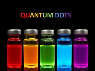
- 4. Quantum Dot Description :- Size, energy level and emission colour can be precisely controlled. Requisite adsorption and resultant emission wavelengths depend on the dot size. The bigger the quantum dots larger the wavelength and smaller is the frequency. The energy band gap increases with the decrease in the size of the quantum dot. Hence more energy is needed to excite the dot and therefore more energy is released when the crystal returns to the resting state.
- 5. Energy Bands Splitting of energy levels in quantum dots due to the quantum confinement effect, semiconductor band gap increases with decrease in size of the nanocrystal..
- 6. SYNTHESIS Quantum dots are synthesized by 3 common methods:- Lithography Colloidal synthesis Epitaxy
- 7. LITHOGRAHY Quantum wells are covered with polymer mask and are exposed to electron or ion beam. The surface is covered with a thin layer of metal and then cleaned and only the exposed areas keep the metal layer .Pillars are etched into the entire surface. Multiple layers are applied this way to build up the properties and size wanted Disadvantages:- slow , possible contamination, low density, defect formation
- 8. COLLOIDAL SYNTHESIS Immersion of semiconductor microcrystals in glass dielectric matrices. Taking a silicate glass with 1% semi conducting phase ( CdS, CdSe, CuCl or CuBr). Heating for several hours at high temperatures. Formation of microcrystals of nearly equal size. Typically group II-VI elements.
- 9. Epitaxy Semiconducting compounds with smaller band gap are grown on the surface of compound with larger band gap. For e.g. GaAs in AlGaAs Growth is restricted by coating it with a masking compound ( Si02) and etching that mask with the shape of required crystal cell well wall shape.
- 10. APPLICATIONS