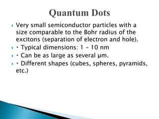
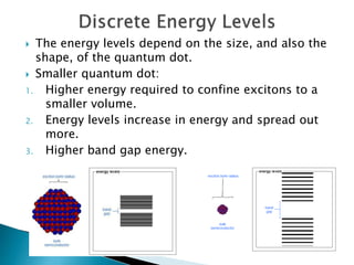
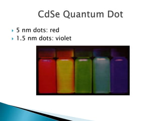
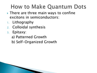
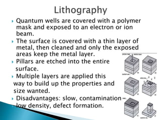
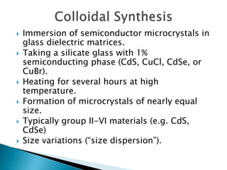
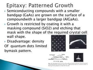
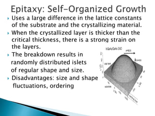
PRESENTED BY:
ASHRAF ALI
DEPARTMENT OF NANOTECHNOLOGY
NEHU,SHILLONG
 Quantum dots (QD) are nanoparticles/structures that
exhibit 3 dimensional quantum confinement, which
leads to many unique optical and transport properties.
 Quantum dots are usually regarded as semiconductors
by definition
 Similar behavior is observed in some metals.
Therefore, in some cases it may be acceptable to speak
about metal quantum dots.
 QDs are band gap tunable by size
which means their optical and electrical
properties can be engineered to meet
specific applications
 Quantum Confinement is the spatial confinement of
electron-hole pairs (excisions) in one or more
dimensions within a material.
◦ 1D confinement: Quantum Wells
◦ 2D confinement: Quantum Wire
◦ 3D confinement: Quantum Dot
 Quantum confinement is more prominent in
semiconductors because they have an energy gap in
their electronic band structure.
 Metals do not have a band gap, so quantum size
effects are less prevalent. Quantum confinement is
only observed at dimensions below 2 nm
 Nanocrystals (2-10 nm) of semiconductor
compounds
 Small size leads to confinement of excitons
(electron-hole pairs)
 Quantized energy levels and altered relaxation
dynamics
 Examples: CdSe, PbSe, PbTe, InP
 Absorption and emission occur at specific
wavelengths, which are related to QD size
 Electrons in conduction band (and holes in
the valence
 band) are free to move in all three
dimensions of space
 Electrons in conduction band (and holes in
the valenceband) are free to move in two
dimensions.
 Confined in one dimension by a potential
well.
 Potential well created due to a larger
bandgap of thesemiconductors on either side
of the thin film.
 Thinner films lead to higher energy levels.
 Thin semiconductor wire surrounded by a
material with a larger bandgap.
 Surrounding material confines electrons and
holes in two dimensions (carriers can only
move in one dimension) due to its larger
bandgap.
 Quantum wire acts as a
potential well.
 Electrons and holes are confined in all three
dimensions of space by a surrounding
material with a larger bandgap.
 Discrete energy levels (artificial atom).
 A quantum dot has a larger bandgap.
 Like bulk semiconductor, electrons tend to
make transitions near the edges of the
bandgap in quantum dots.
 Very small semiconductor particles with a
size comparable to the Bohr radius of the
excitons (separation of electron and hole).
 Typical dimensions: 1 – 10 nm
 Can be as large as several μm.
 Different shapes (cubes, spheres, pyramids,
etc.)
 The energy levels depend on the size, and also the
shape, of the quantum dot.
 Smaller quantum dot:
1. Higher energy required to confine excitons to a
smaller volume.
2. Energy levels increase in energy and spread out
more.
3. Higher band gap energy.
 5 nm dots: red
 1.5 nm dots: violet
 There are three main ways to confine
excitons in semiconductors:
1. Lithography
2. Colloidal synthesis
3. Epitaxy:
a) Patterned Growth
b) Self-Organized Growth
 Quantum wells are covered with a polymer
mask and exposed to an electron or ion
beam.
 The surface is covered with a thin layer of
metal, then cleaned and only the exposed
areas keep the metal layer.
 Pillars are etched into the entire
surface.
 Multiple layers are applied this
way to build up the properties and
size wanted.
 Disadvantages: slow, contamination,
 low density, defect formation.
 Immersion of semiconductor microcrystals in
glass dielectric matrices.
 Taking a silicate glass with 1%
semiconducting phase (CdS, CuCl, CdSe, or
CuBr).
 Heating for several hours at high
temperature.
 Formation of microcrystals of nearly equal
size.
 Typically group II-VI materials (e.g. CdS,
CdSe)
 Size variations (“size dispersion”).
 Semiconducting compounds with a smaller
bandgap (GaAs) are grown on the surface of a
compoundwith a larger bandgap (AlGaAs).
 Growth is restricted by coating it with a
masking compound (SiO2) and etching that
mask with the shape of the required crystal cell
wall shape.
 Disadvantage: density
Of quantum dots limited
bymask pattern.
 Uses a large difference in the lattice constants
of the substrate and the crystallizing material.
 When the crystallized layer is thicker than the
critical thickness, there is a strong strain on
the layers.
 The breakdown results in
randomly distributed islets
of regular shape and size.
 Disadvantages: size and shape
fluctuations, ordering
 In many regions of the world there is now, or
soon to be, legislation to restrict and in some
cases ban heavy metals in many household
appliances such as IT & telecommunication
equipment, Lighting equipment , Electrical &
electronic tools, Toys, leisure & sports
equipment.
 For QDs to be commercially viable in many
applications they MUST NOT CONTAIN
cadmium or other restricted elements LIKE
mercury, lead, chromium.
 So research has been able to create non-toxic
quantum dots using silicon.
 Very narrow spectral line width, depending on
the quantum dot’s size.
 Multiplexed detection
 Large absorption coefficients across a wide
spectral range.
 Small size / high surface-to-volume ratio.
 Very high levels of brightness.
 Blinking.
 Photovoltaic devices: solar cells
 Biology : biosensors, imaging
 Light emitting diodes: LEDs
 Quantum computation
 Flat-panel displays
 Memory elements
 Photodetectors
 Lasers
THANK YOU

Quantum dots 1

  • 1.
    PRESENTED BY: ASHRAF ALI DEPARTMENTOF NANOTECHNOLOGY NEHU,SHILLONG
  • 2.
     Quantum dots(QD) are nanoparticles/structures that exhibit 3 dimensional quantum confinement, which leads to many unique optical and transport properties.  Quantum dots are usually regarded as semiconductors by definition  Similar behavior is observed in some metals. Therefore, in some cases it may be acceptable to speak about metal quantum dots.  QDs are band gap tunable by size which means their optical and electrical properties can be engineered to meet specific applications
  • 3.
     Quantum Confinementis the spatial confinement of electron-hole pairs (excisions) in one or more dimensions within a material. ◦ 1D confinement: Quantum Wells ◦ 2D confinement: Quantum Wire ◦ 3D confinement: Quantum Dot  Quantum confinement is more prominent in semiconductors because they have an energy gap in their electronic band structure.  Metals do not have a band gap, so quantum size effects are less prevalent. Quantum confinement is only observed at dimensions below 2 nm
  • 4.
     Nanocrystals (2-10nm) of semiconductor compounds  Small size leads to confinement of excitons (electron-hole pairs)  Quantized energy levels and altered relaxation dynamics  Examples: CdSe, PbSe, PbTe, InP  Absorption and emission occur at specific wavelengths, which are related to QD size
  • 5.
     Electrons inconduction band (and holes in the valence  band) are free to move in all three dimensions of space
  • 6.
     Electrons inconduction band (and holes in the valenceband) are free to move in two dimensions.  Confined in one dimension by a potential well.  Potential well created due to a larger bandgap of thesemiconductors on either side of the thin film.  Thinner films lead to higher energy levels.
  • 7.
     Thin semiconductorwire surrounded by a material with a larger bandgap.  Surrounding material confines electrons and holes in two dimensions (carriers can only move in one dimension) due to its larger bandgap.  Quantum wire acts as a potential well.
  • 8.
     Electrons andholes are confined in all three dimensions of space by a surrounding material with a larger bandgap.  Discrete energy levels (artificial atom).  A quantum dot has a larger bandgap.  Like bulk semiconductor, electrons tend to make transitions near the edges of the bandgap in quantum dots.
  • 9.
     Very smallsemiconductor particles with a size comparable to the Bohr radius of the excitons (separation of electron and hole).  Typical dimensions: 1 – 10 nm  Can be as large as several μm.  Different shapes (cubes, spheres, pyramids, etc.)
  • 10.
     The energylevels depend on the size, and also the shape, of the quantum dot.  Smaller quantum dot: 1. Higher energy required to confine excitons to a smaller volume. 2. Energy levels increase in energy and spread out more. 3. Higher band gap energy.
  • 11.
     5 nmdots: red  1.5 nm dots: violet
  • 12.
     There arethree main ways to confine excitons in semiconductors: 1. Lithography 2. Colloidal synthesis 3. Epitaxy: a) Patterned Growth b) Self-Organized Growth
  • 13.
     Quantum wellsare covered with a polymer mask and exposed to an electron or ion beam.  The surface is covered with a thin layer of metal, then cleaned and only the exposed areas keep the metal layer.  Pillars are etched into the entire surface.  Multiple layers are applied this way to build up the properties and size wanted.  Disadvantages: slow, contamination,  low density, defect formation.
  • 14.
     Immersion ofsemiconductor microcrystals in glass dielectric matrices.  Taking a silicate glass with 1% semiconducting phase (CdS, CuCl, CdSe, or CuBr).  Heating for several hours at high temperature.  Formation of microcrystals of nearly equal size.  Typically group II-VI materials (e.g. CdS, CdSe)  Size variations (“size dispersion”).
  • 15.
     Semiconducting compoundswith a smaller bandgap (GaAs) are grown on the surface of a compoundwith a larger bandgap (AlGaAs).  Growth is restricted by coating it with a masking compound (SiO2) and etching that mask with the shape of the required crystal cell wall shape.  Disadvantage: density Of quantum dots limited bymask pattern.
  • 16.
     Uses alarge difference in the lattice constants of the substrate and the crystallizing material.  When the crystallized layer is thicker than the critical thickness, there is a strong strain on the layers.  The breakdown results in randomly distributed islets of regular shape and size.  Disadvantages: size and shape fluctuations, ordering
  • 17.
     In manyregions of the world there is now, or soon to be, legislation to restrict and in some cases ban heavy metals in many household appliances such as IT & telecommunication equipment, Lighting equipment , Electrical & electronic tools, Toys, leisure & sports equipment.  For QDs to be commercially viable in many applications they MUST NOT CONTAIN cadmium or other restricted elements LIKE mercury, lead, chromium.  So research has been able to create non-toxic quantum dots using silicon.
  • 18.
     Very narrowspectral line width, depending on the quantum dot’s size.  Multiplexed detection  Large absorption coefficients across a wide spectral range.  Small size / high surface-to-volume ratio.  Very high levels of brightness.  Blinking.
  • 19.
     Photovoltaic devices:solar cells  Biology : biosensors, imaging  Light emitting diodes: LEDs  Quantum computation  Flat-panel displays  Memory elements  Photodetectors  Lasers
  • 20.