Downloaded 284 times
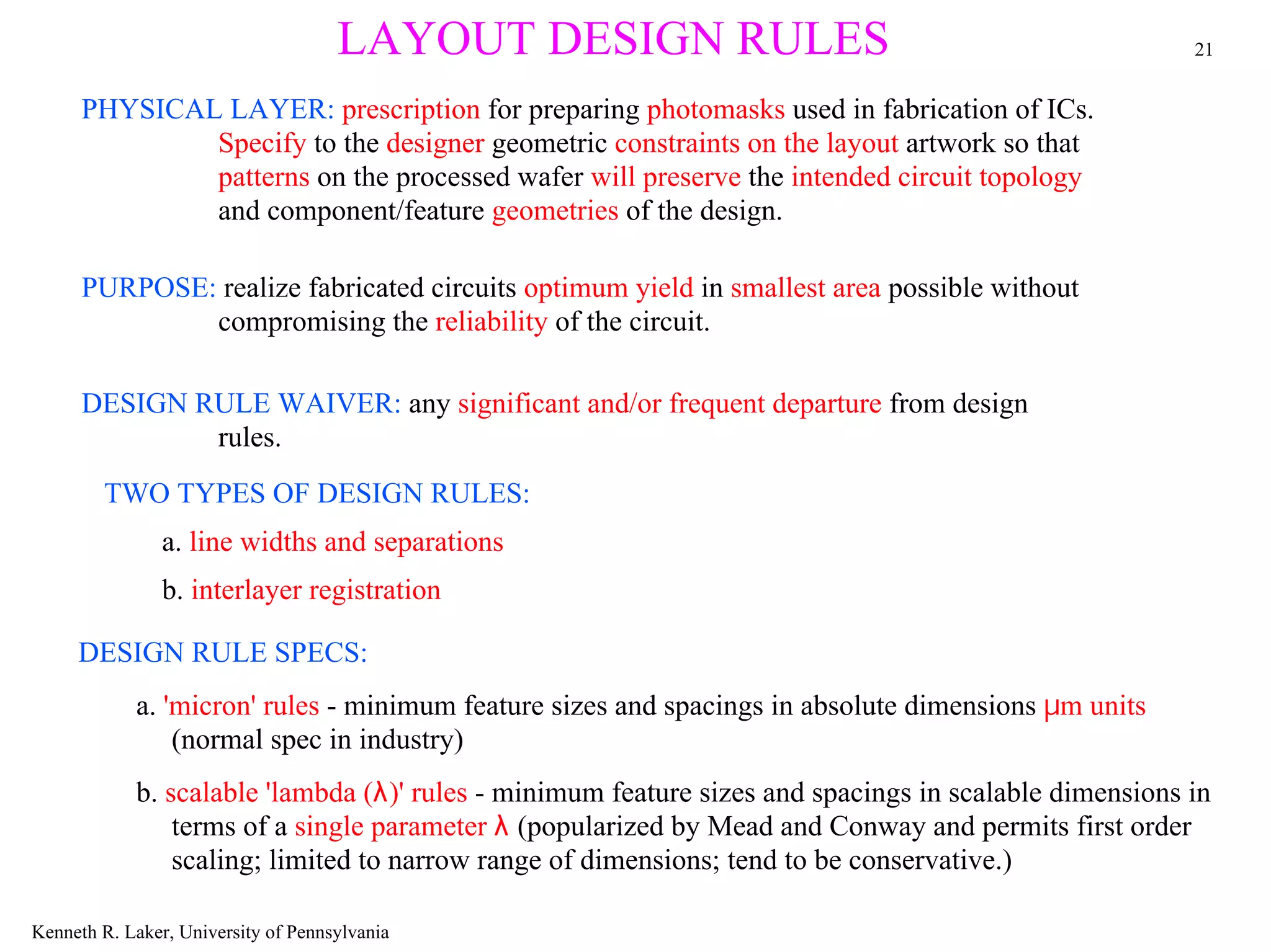
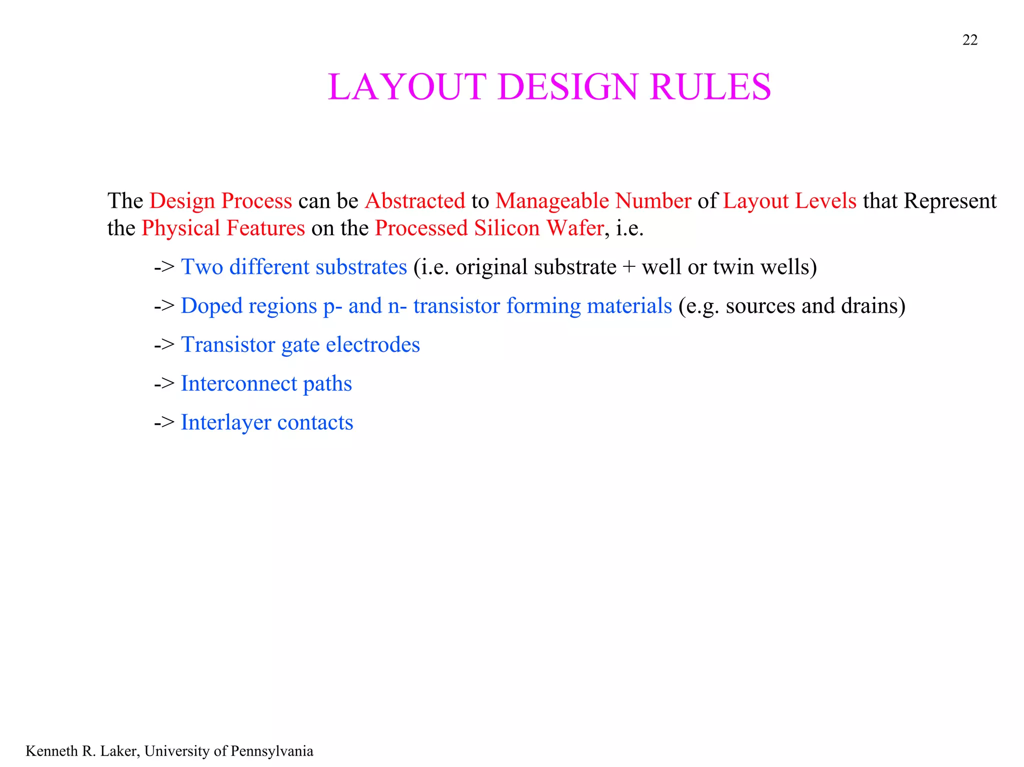
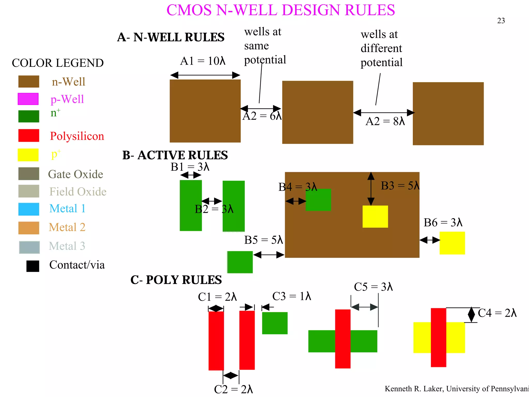
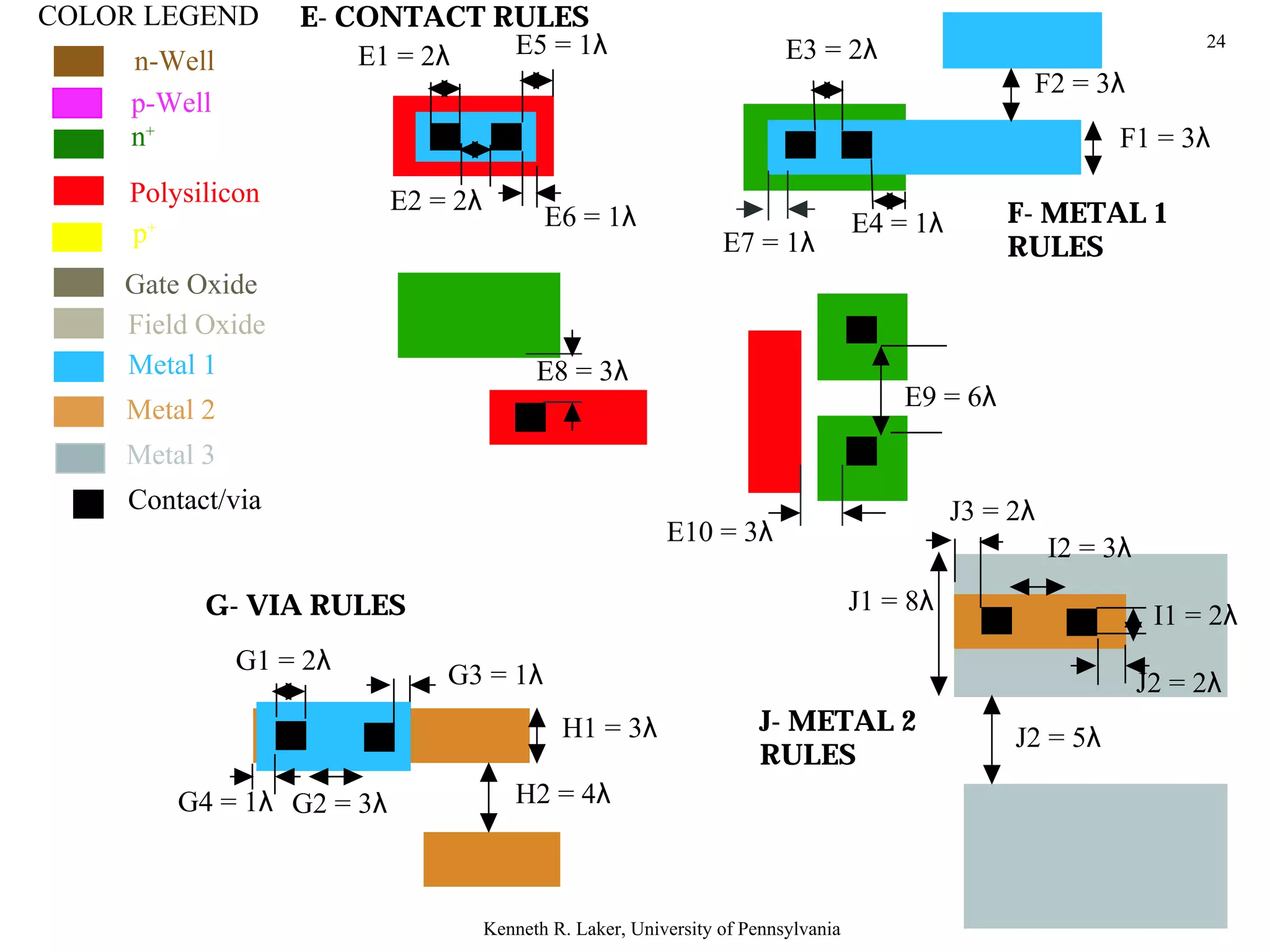
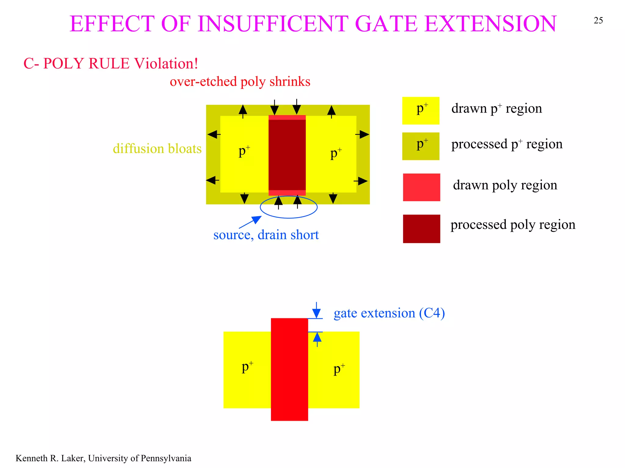
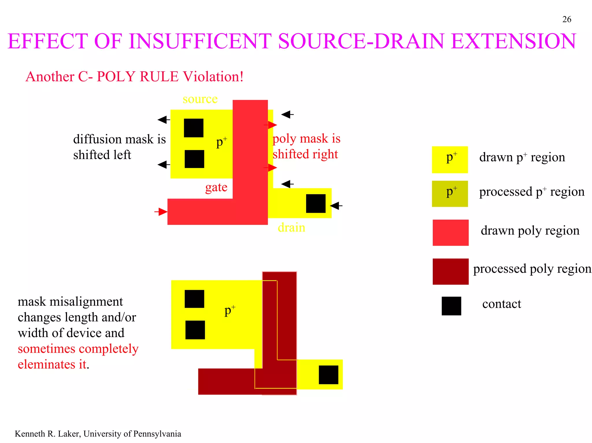
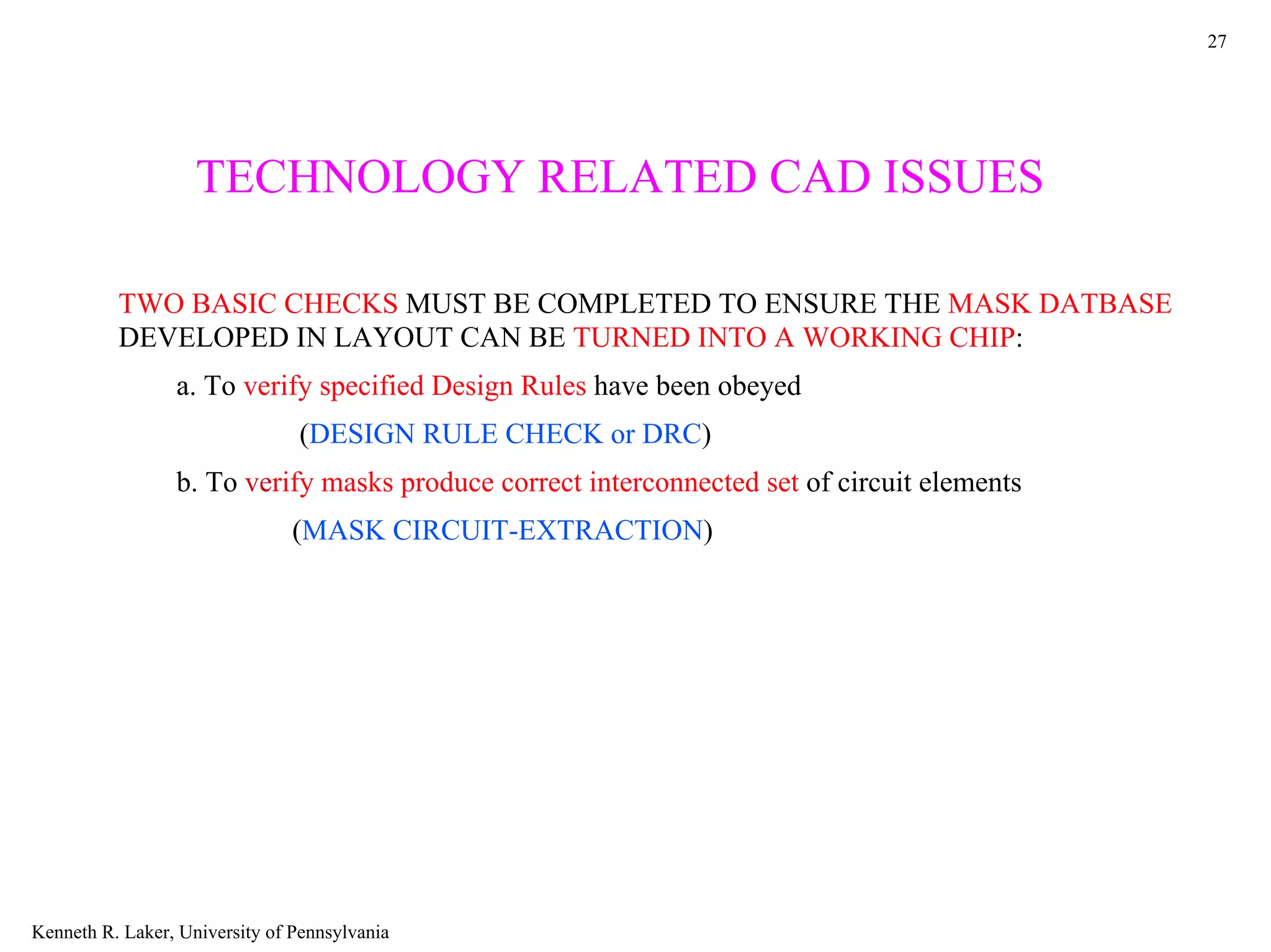
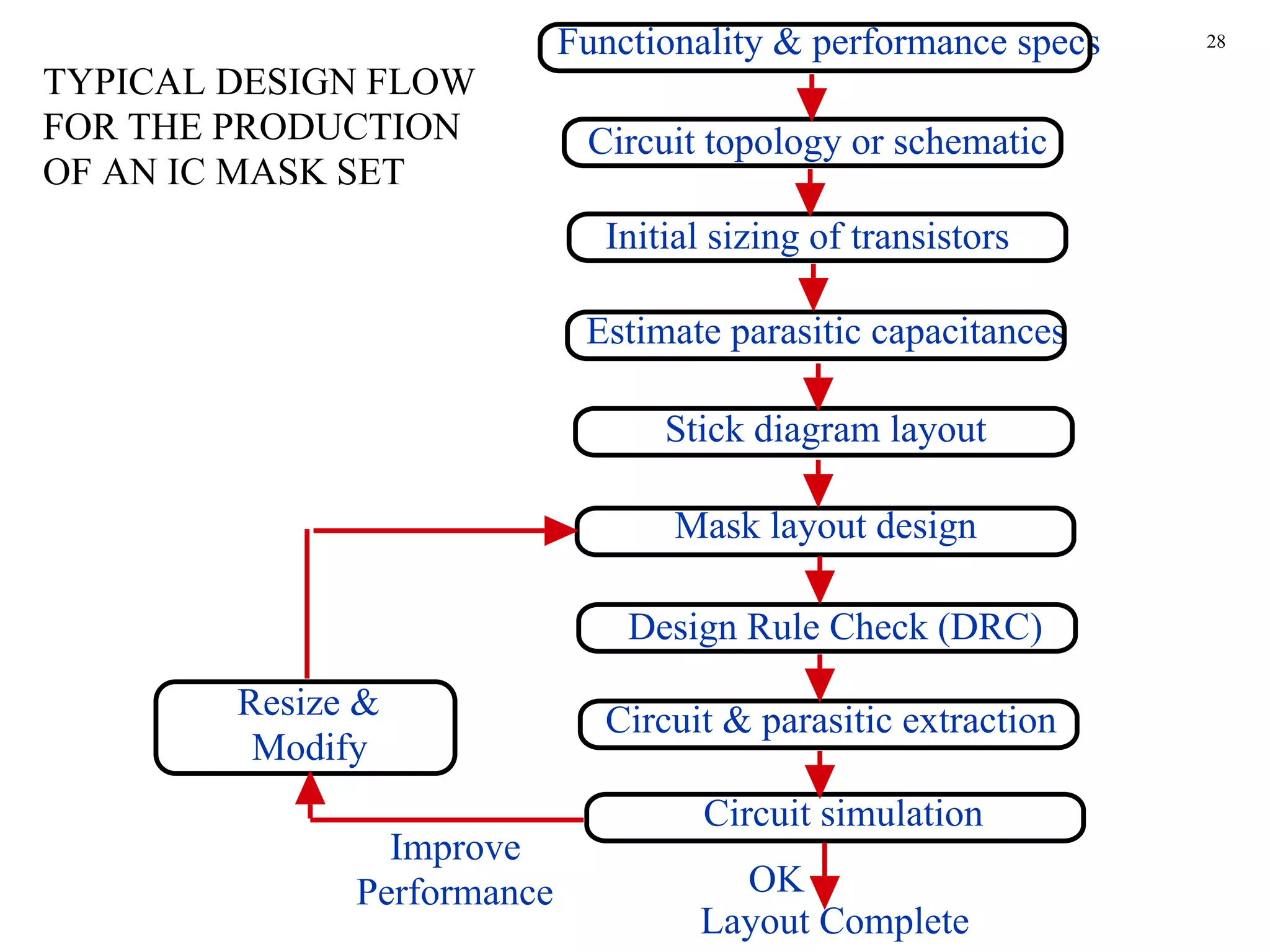

The document discusses layout design rules for integrated circuits. It provides guidelines for feature sizes and spacings to ensure fabricated circuits meet intended designs. This includes minimum line widths, separations between layers, and allowances for misalignment. The document also notes two key checks that must be completed to validate a mask design: a design rule check to verify rules are followed, and circuit extraction to confirm masks produce the correct interconnected circuit.


