Download as PPSX, PPTX


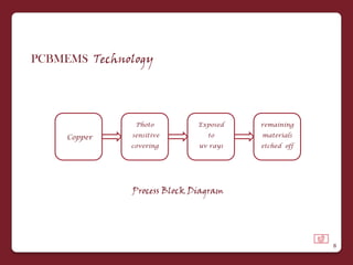


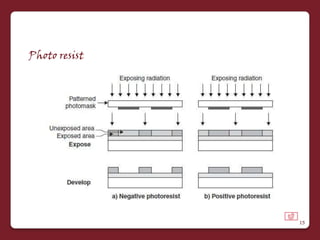
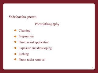
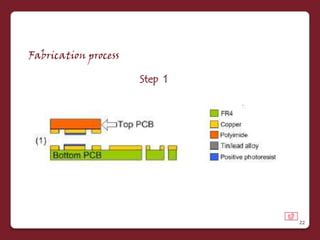
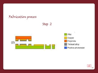
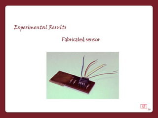
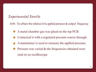
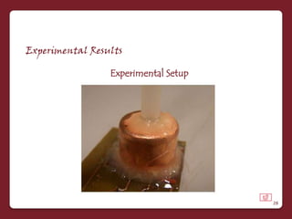
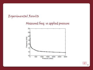
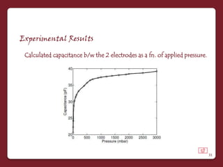

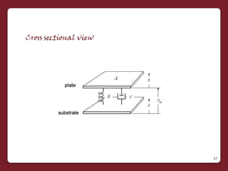


This document summarizes the design, fabrication process, and experimental results of a capacitive pressure sensor made using printed circuit board microelectromechanical systems (PCBMEMS) technology. The sensor consists of two FR4 circuit boards with a small separation that varies with applied pressure, changing the capacitance. Photolithography is used to etch copper patterns on the boards. Experimental results show the sensor's output frequency varies linearly with increasing applied pressure up to 3,000 mbar. The low-cost PCBMEMS fabrication process could enable integration with electronics for pressure sensing in various industries.


