The document discusses the design and analysis of a D-flip flop. It begins by introducing flip flops and their use for storing state information. It then discusses the need for a D-flip flop due to limitations in the basic SR flip flop. A D-flip flop overcomes these limitations using a gated SR flip flop with an inverter between the S and R inputs, allowing a single data input. The circuit and working of the D-flip flop are shown, noting it will store and output the data input while the clock is high.
Laxmi Narain Collegeof Technology
Indore
PRESENTATION ON
“ DESIGN AND ANALYSIS OF
D-FLIP FLOP ”
Submitted to : Submitted by :
Er. Deepak Sir Pradhan Rishi Sharma
Prem Gour
Pragya jain
2.
Introduction to FlipFlop
●
A flip-flop or latch is a circuit that has two stable states
and can be used to store state information
● It is the basic storage element in sequential logic
● A flip-flop stores a single bit (binary digit) of data; one
of its two states represents a "one" and the other
represents a "zero"
( OR )
Flip-flops maintain their state until an input pulse called a
trigger is received. When a trigger is received, the flip-flop
outputs change state according to defined rules and remain in
those states until another trigger is received
3.
The Need ofD flip flop
One of the main disadvantages of the basic SR
flip flop circuit is that the indeterminate input
condition of "SET" = logic "0" and "RESET" =
logic "0" is forbidden.
In Simpler words , When R=S=0 or R=S=1 , the
outputs Q and Q' either don't change or they are
indeterminate(Invalid)
4.
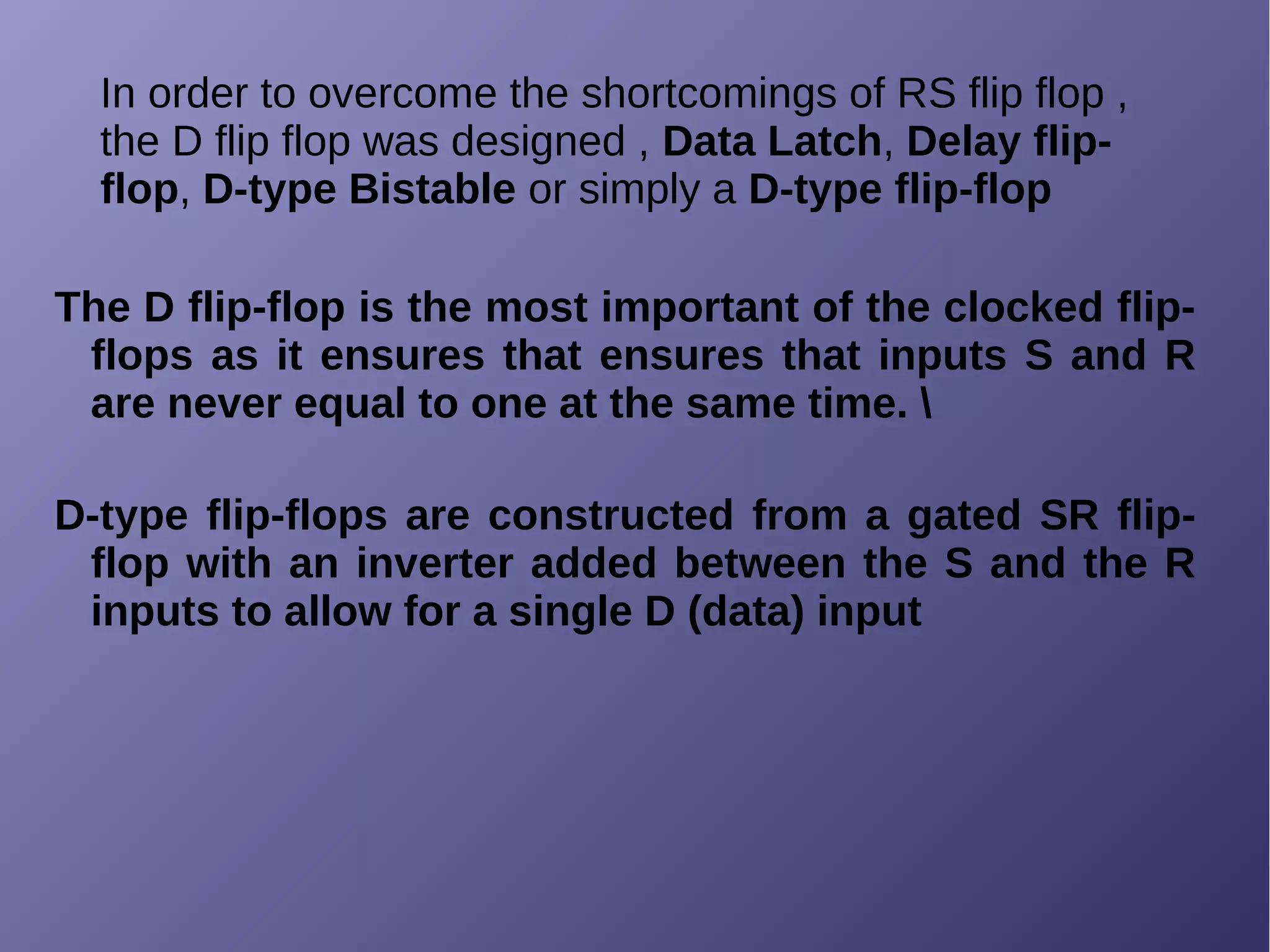
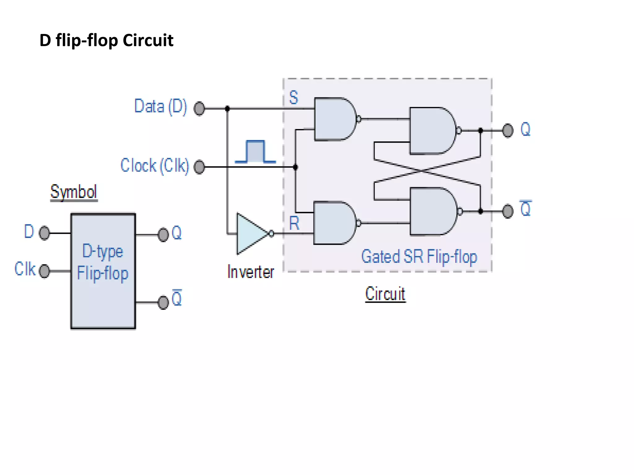
In order toovercome the shortcomings of RS flip flop ,
the D flip flop was designed , Data Latch, Delay flip-
flop, D-type Bistable or simply a D-type flip-flop
The D flip-flop is the most important of the clocked flip-
flops as it ensures that ensures that inputs S and R
are never equal to one at the same time.
D-type flip-flops are constructed from a gated SR flip-
flop with an inverter added between the S and the R
inputs to allow for a single D (data) input
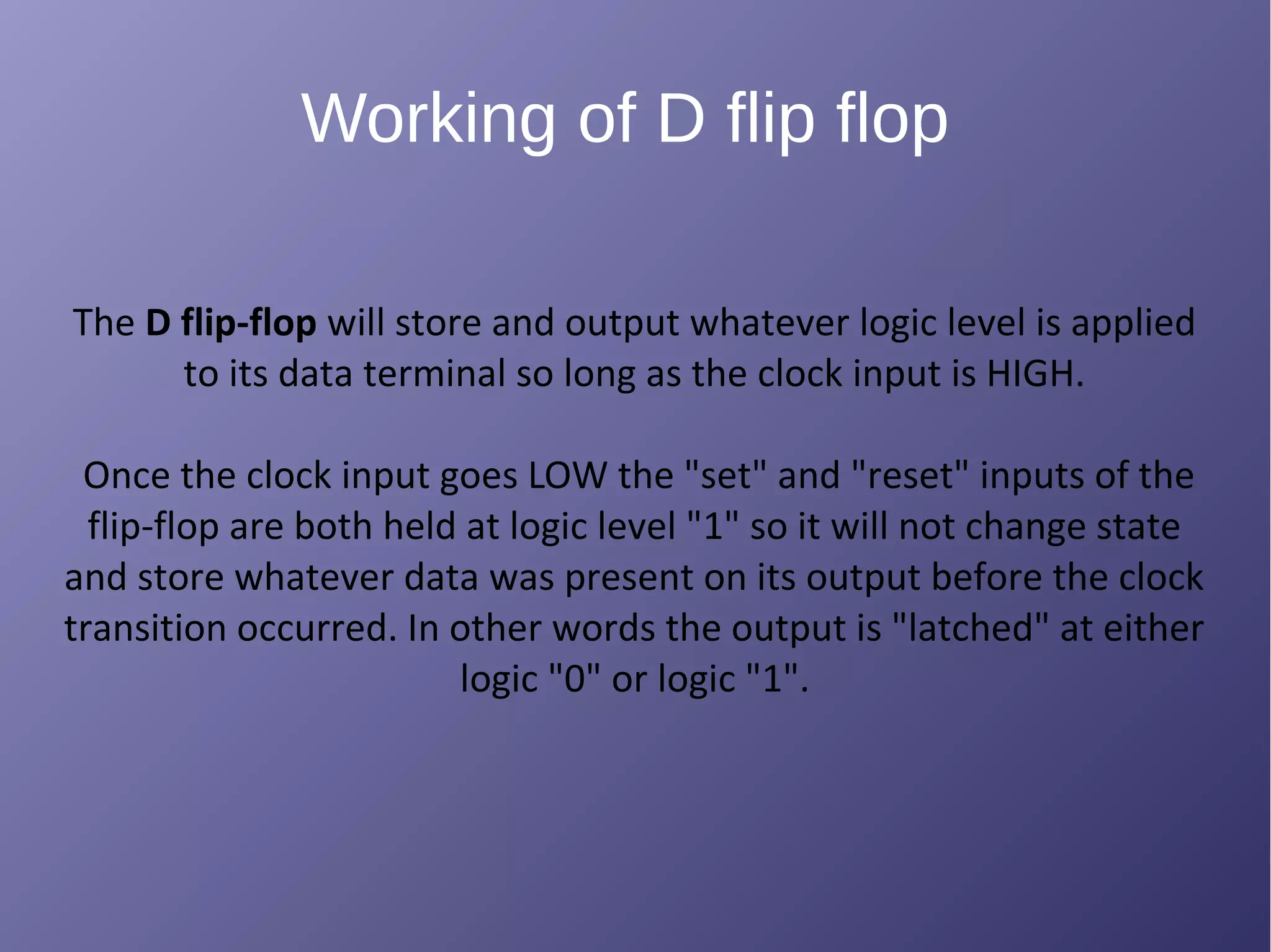
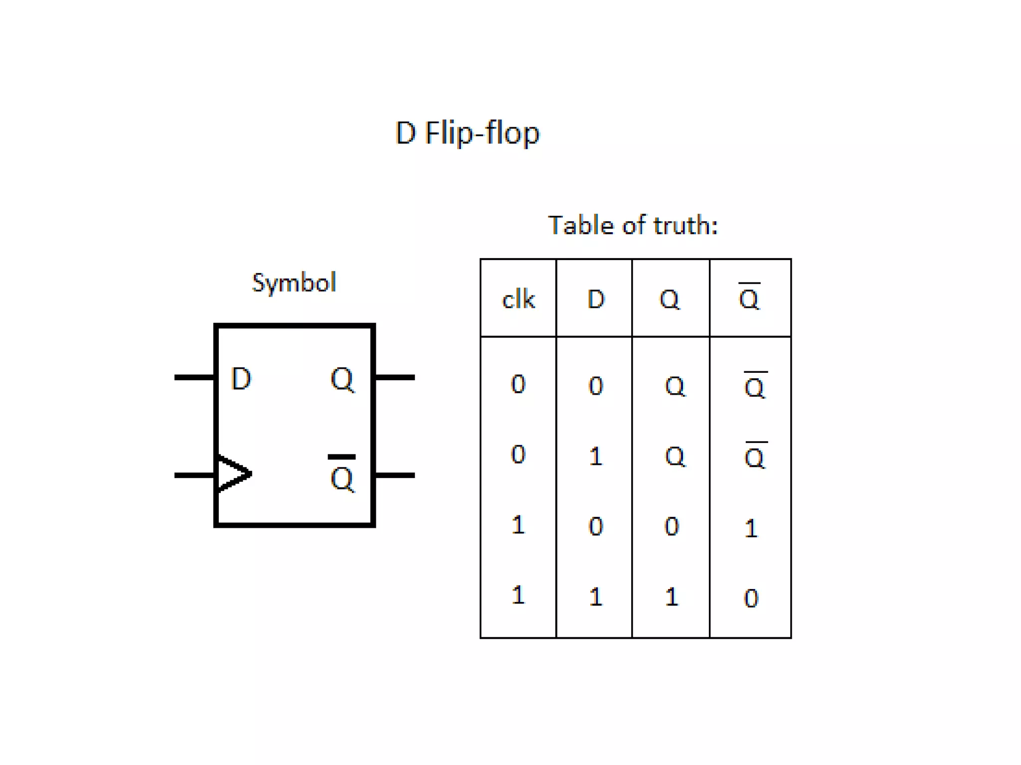
Working of Dflip flop
The D flip-flop will store and output whatever logic level is applied
to its data terminal so long as the clock input is HIGH.
Once the clock input goes LOW the "set" and "reset" inputs of the
flip-flop are both held at logic level "1" so it will not change state
and store whatever data was present on its output before the clock
transition occurred. In other words the output is "latched" at either
logic "0" or logic "1".
8.
The D-type FlipFlop Summary
The data or D-type Flip Flop can be built using a
pair of back-to-back SR latches and connecting
an inverter (NOT Gate) between the S and the R
inputs to allow for a single D (data) input. The
basic D flip flop circuit can be improved further by
adding a second SR flip-flop to its output that is
activated on the complementary clock signal to
produce a “Master-Slave D flip-flop” device.


![SEQUENTIAL CIRCUITS [Flip-flops and Latches]](https://cdn.slidesharecdn.com/ss_thumbnails/sequentialcircuits-211217082412-thumbnail.jpg?width=640&height=640&fit=bounds)


![Flip_flops_in_digital_electronics[1].pptx](https://cdn.slidesharecdn.com/ss_thumbnails/flipflopsindigitalelectronics1-250805201548-623d4f88-thumbnail.jpg?width=640&height=640&fit=bounds)
![Flip_flops_in_digital_electronics[1].pptx](https://cdn.slidesharecdn.com/ss_thumbnails/flipflopsindigitalelectronics1-250805201909-5c7c72ae-thumbnail.jpg?width=640&height=640&fit=bounds)