Digital logic Presentation flipflop and latches.pptx
1.
1
FLIP-FLOPS VS. LATCHES:EDGE-TRIGGERING
VS. LEVEL-TRIGGERING
- COMPARISON OF RS, JK, D, AND T FLIPFLOPS WITH TIMING DIAGRAMS
Presenter Name: Golu Kohar and Aastha Sherchan
2.
2
Latches aredigital circuits that store a single bit of information and hold its value
until it is updated by new input signals.
Latches are widely used in data storage, control circuits, and flip-flop circuits.
A latch is also called bi-stable has two stable states, one state is referred to
as set and the other as reset.
TYPES OF LATCHES:
SR Latches
Gated SR Latches
D Latches
Gated D Latches
JK Latches
T Laches
LATCHES
3.
3
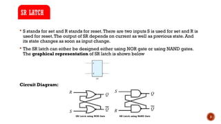
S standsfor set and R stands for reset.There are two inputs S is used for set and R is
used for reset.The output of SR depends on current as well as previous state. And
its state changes as soon as input change.
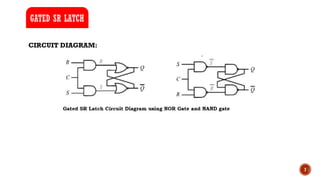
The SR latch can either be designed either using NOR gate or using NAND gates.
The graphical representation of SR latch is shown below
Circuit Diagram:
SR LATCH
4.
4
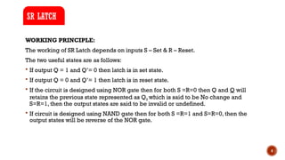
WORKING PRINCIPLE:
The workingof SR Latch depends on inputs S – Set & R – Reset.
The two useful states are as follows:
If output Q = 1 and Q’= 0 then latch is in set state.
If output Q = 0 and Q’= 1 then latch is in reset state.
If the circuit is designed using NOR gate then for both S =R=0 then Q and Q will
retains the previous state represented as Q0 which is said to be No change and
S=R=1, then the output states are said to be invalid or undefined.
If circuit is designed using NAND gate then for both S =R=1 and S=R=0, then the
output states will be reverse of the NOR gate.
SR LATCH
5.
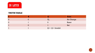
5
S R QState
0 0 Q0 No Change
0 1 0 Reset
1 0 1 Set
1 1 Q = Q = Invalid
SR LATCH
TRUTH TABLE
6.
6
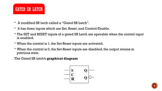
A modifiedSR latch called a “Gated SR Latch”.
It has three inputs which are Set, Reset, and Control/Enable.
The SET and RESET inputs of a gated SR Latch are operable when the control input
is enabled.
When the control is 1, the Set-Reset inputs are activated.
When the control is 0, the Set-Reset inputs are disabled, the output retains in
previous state.
The Gated SR latch’s graphical diagram
GATED SR LATCH
8
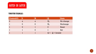
TRUTH TABLE:
GATED SRLATCH
Control(C) S R Q State
0 x x Q0 No change
1 0 0 Q0 Nochange
1 0 1 0 Reset
1 1 0 1 Set
1 1 1 Q = Q = Invalid
9.
9
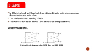
In SRLatch, when S and R are both 1, we obtained invalid state where we cannot
determine the next state value.
This can be modified by using D latch.
The D latch is also called as Data Latch or Delay or Transparent latch.
CIRCUIT DIAGRAM:
D LATCH
10.
10
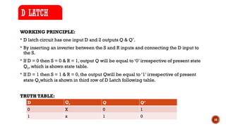
WORKING PRINCIPLE:
Dlatch circuit has one input D and 2 outputs Q & Q’.
By inserting an inverter between the S and R inputs and connecting the D input to
the S.
If D = 0 then S = 0 & R = 1, output Q will be equal to ‘0’ irrespective of present state
Q0, which is shown state table.
If D = 1 then S = 1 & R = 0, the output Qwill be equal to ‘1’ irrespective of present
state Q0which is shown in third row of D Latch following table.
TRUTH TABLE:
D LATCH
D Qo Q Q’
0 X 0 1
1 x 1 0
11.
11
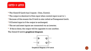
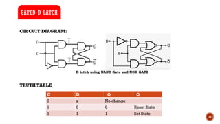
The GatedD Latch has 2 inputs – Data, Control.
The output is identical to Data input when control input is set to 1.
Because of this reason the D latch is also called as Transparent Latch.
If Control input is 0 the output is unchanged.
The set and reset inputs are connected via an inverter.
If this is done, the output will be opposite to one another.
The Gated D latch’s graphical diagram
GATED D LATCH
13
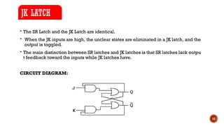
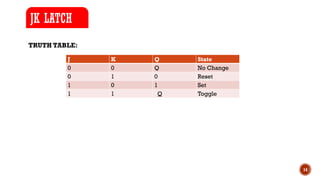
The SRLatch and the JK Latch are identical.
When the JK inputs are high, the unclear states are eliminated in a JK latch, and the
output is toggled.
The main distinction between SR latches and JK latches is that SR latches lack outpu
t feedback toward the inputs while JK latches have.
CIRCUIT DIAGRAM:
JK LATCH
15
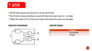
The JKlatch inputs are shorted to create the T latch.
The T latch’s output switches on and off when the input is set to 1 or high.
.When the input of T is 0 then the output will retain the same (no change).
CIRCUIT DIAGRAM TRUTH TABLE
T LATCH
T Output
0 No Change
1 Toggle
16.
16
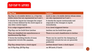
FLIP-FLOP VS LATCHES
Flip-FlopLatches
flip-flop is a bi-stable device i.e., it has two
stable states that are represented as 0 and 1.
Latch is also a bi-stable device whose states
are also represented as 0 and 1.
It checks the inputs but changes the output
only at times defined by the clock signal or
any other control signal.
It checks the inputs continuously and
responds to the changes in inputs
immediately.
It is a edge triggered device. It is a level triggered device
Flip-flop can be build from Latches Latches can be build from gates.
They are classified into asynchronous or
synchronous flip-flops.
There is no such classification in latches
It forms the building blocks of many
sequential circuits like counters.
These can be used for the designing of
sequential circuits but are not generally
preferred.
Flip-flop always have a clock signal Latches doesn't have a clock signal
ex: D Flip-flop, JK Flip-flop ex: SR Latch, D Latch
17.
17
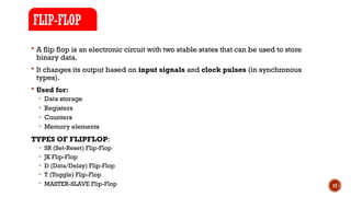
A flipflop is an electronic circuit with two stable states that can be used to store
binary data.
It changes its output based on input signals and clock pulses (in synchronous
types).
Used for:
• Data storage
• Registers
• Counters
• Memory elements
TYPES OF FLIPFLOP:
• SR (Set-Reset) Flip-Flop
• JK Flip-Flop
• D (Data/Delay) Flip-Flop
• T (Toggle) Flip-Flop
• MASTER-SLAVE Flip-Flop
FLIP-FLOP
18.
18
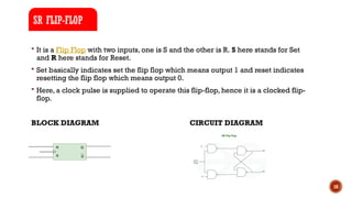
It isa Flip Flop with two inputs, one is S and the other is R. S here stands for Set
and R here stands for Reset.
Set basically indicates set the flip flop which means output 1 and reset indicates
resetting the flip flop which means output 0.
Here, a clock pulse is supplied to operate this flip-flop, hence it is a clocked flip-
flop.
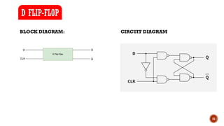
BLOCK DIAGRAM CIRCUIT DIAGRAM
SR FLIP-FLOP
19.
19
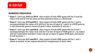
WORKING PRINCIPLE:
Case1 : Let's say, S=0 and R=0 , then output of both AND gates will be 0 and the
value of Q and Q' will be same as their previous value, i.e, Hold state.
Case 2 : Let's say, S=0 and R=1 , then output of both AND gates will be 1 and 0,
correspondingly the value of Q will be 0 as one of input is 1 and it is a NOR gate so
it will ultimately gives 0, hence Q gets 0 value, similarly Q' will be 1.
Case 3 : Let's say, S=1 and R=0 , then output of both AND gates will be 0 and 1,
correspondingly the value of Q' will be 0 as one of input to NOR gate is 1, so output
will be 0 ultimately and this 0 value will go as input to upper NOR gate, and hence
Q will become 1.
Case 4 : Let's say, S=1 and R=1 , then output of both AND gates will be 1 and 1
which is invalid, as the outputs should be complement of each other.
SR FLIP-FLOP
20.
20
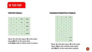
TRUTH TABLE: CHARACTERISTICSTABLE:
SR FLIP-FLOP
Here, S is the Set input, R is the reset
input,Qn+1 is the next state
and State tells in which state it enters
Here, S is the Set input, R is the reset
input, Qn is the current state input
and Qn+1 is the next state outputs.
21.
21
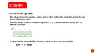
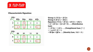
Characteristic Equation:
Thecharacteristic equation tells us about what will be the next state of flip flop in
terms of present state.
In order to get the characteristic equation, K-Map is constructed which will be
shown as below:
If we solve the above K-Map then the characteristic equation will be:
Qn+1 = S + QnR’
SR FLIP-FLOP
22.
22
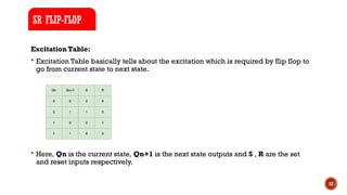
Excitation Table:
ExcitationTable basically tells about the excitation which is required by flip flop to
go from current state to next state.
Here, Qn is the current state, Qn+1 is the next state outputs and S , R are the set
and reset inputs respectively.
SR FLIP-FLOP
24
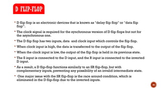
D flipflop is an electronic devices that is known as "delay flip flop" or "data flip
flop“.
The clock signal is required for the synchronous version of D flip flops but not for
the asynchronous one.
The D flip flop has two inputs, data and clock input which controls the flip flop.
When clock input is high, the data is transferred to the output of the flip flop.
When the clock input is low, the output of the flip flop is held in its previous state.
The S input is connected to the D input, and the R input is connected to the inverted
D input.
As a result, a D flip-flop functions similarly to an SR flip-flop, but with
complementary inputs, preventing any possibility of an invalid intermediate state.
One major issue with the SR flip-flop is the race around condition, which is
eliminated in the D flip-flop due to the inverted inputs.
D FLIP-FLOP
26
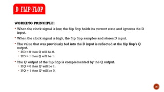
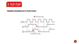
WORKING PRINCIPLE:
Whenthe clock signal is low, the flip flop holds its current state and ignores the D
input.
When the clock signal is high, the flip flop samples and stores D input.
The value that was previously fed into the D input is reflected at the flip flop's Q
output.
• If D = 0 then Q will be 0.
• If D = 1 then Q will be 1.
The Q' output of the flip flop is complemented by the Q output.
• If Q = 0 then Q' will be 1.
• If Q = 1 then Q' will be 0.
D FLIP-FLOP
27.
27
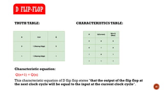
TRUTH TABLE: CHARACTERISTICSTABLE:
Characteristic equation:
Q(n+1) = Q(n)
This characteristic equation of D flip flop states "that the output of the flip flop at
the next clock cycle will be equal to the input at the current clock cycle".
D FLIP-FLOP
28.
28
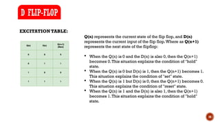
EXCITATION TABLE:
D FLIP-FLOP
Q(n)represents the current state of the flip flop, and D(n)
represents the current input of the flip flop.Where as Q(n+1)
represents the next state of the flipflop:
When the Q(n) is 0 and the D(n) is also 0, then the Q(n+1)
becomes 0.This situation explains the condition of "hold"
state.
When the Q(n) is 0 but D(n) is 1, then the Q(n+1) becomes 1.
This situation explains the condition of "set" state.
When the Q(n) is 1 but D(n) is 0, then the Q(n+1) becomes 0.
This situation explains the condition of "reset" state.
When the Q(n) is 1 and the D(n) is also 1, then the Q(n+1)
becomes 1.This situation explains the condition of "hold"
state.
30
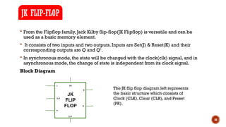
From theFlipflop family, Jack Kilby flip-flop(JK Flipflop) is versatile and can be
used as a basic memory element.
It consists of two inputs and two outputs. Inputs are Set(J) & Reset(K) and their
corresponding outputs are Q and Q‘.
In synchronous mode, the state will be changed with the clock(clk) signal, and in
asynchronous mode, the change of state is independent from its clock signal.
Block Diagram
JK FLIP-FLOP
The JK flip flop diagram left represents
the basic structure which consists of
Clock (CLK), Clear (CLR), and Preset
(PR).
32
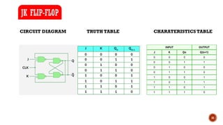
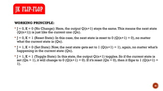
WORKING PRINCIPLE:
J= 0, K = 0 (No Change): Here, the output Q(n+1) stays the same.This means the next state
(Q(n+1)) is just like the current one (Qn).
J = 0, K = 1 (Reset State): In this case, the next state is reset to 0 (Q(n+1) = 0), no matter
what the current state is (Qn).
J = 1, K = 0 (Set State): Now, the next state gets set to 1 (Q(n+1) = 1), again, no matter what’s
happening in the current state (Qn).
J = 1, K = 1 (Toggle State): In this state, the output Q(n+1) toggles. So if the current state is
set (Qn = 1), it will change to 0 (Q(n+1) = 0). If it’s reset (Qn = 0), then it flips to 1 (Q(n+1) =
1).
JK FLIP-FLOP
34
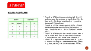
EXCITATION TABLE:
JK FLIP-FLOP
From 0 to 0:When the current state is 0 (Qn = 0)
and you want the next one to stay 0 (Q(n+1) = 0),
then set J = 0 & K can be either 0 or 1, which is
shown as X (Don’t Care).
From 0 to 1: If the current state is 0 (Qn = 0) but
you want the next state to flip to 1 (Q(n+1) = 1),
then J should be set to 1 & K = X (doesn't matter
for K).
From 1 to 0:When you start with a current state of
1 (Qn = 1) & wish for it to switch to 0 (Q(n+1) =
0), then J should be X and K must be set at 1.
From 1 to 1: If you're at a current state of 1 (Qn =
1) & want it to stay at 1 for the next state (Q(n+1)
= 1), then just set J = X and K should be set at 0.
36
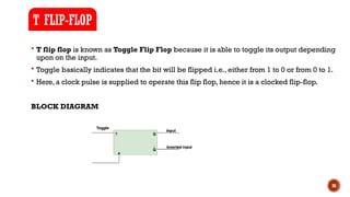
T flipflop is known as Toggle Flip Flop because it is able to toggle its output depending
upon on the input.
Toggle basically indicates that the bit will be flipped i.e., either from 1 to 0 or from 0 to 1.
Here, a clock pulse is supplied to operate this flip flop, hence it is a clocked flip-flop.
BLOCK DIAGRAM
T FLIP-FLOP
37.
37
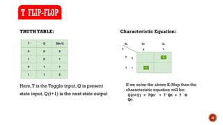
TRUTH TABLE: CharacteristicEquation:
Here,T is the Toggle input, Q is present
state input, Q(t+1) is the next state output
T FLIP-FLOP
If we solve the above K-Map then the
characteristic equation will be:
Q(n+1) = TQn’ + T’Qn = T ⊕
Qn
38.
38
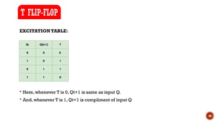
EXCITATION TABLE:
Here,whenever T is 0, Qt+1 is same as input Q.
And, whenever T is 1, Qt+1 is compliment of input Q
T FLIP-FLOP
39.
39
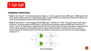
WORKING PRINCIPLE:
Case1: Let's say,T = 0 and clock pulse is high i.e, 1, then output of both, AND gate 1, AND gate 2 will
be 0, gate 3 output will be Q and similarly gate 4 output will be Q' so both the values of Q and Q' are
same as their previous value, which means Hold state.
Case 2: Let's say,T=1, then output of both AND gate 1 will be (T * clock * Q), and since T and clock
both are 1, then the output of AND gate 1 will be Q, and similarly output of AND gate 2 will be (T *
clock * Q') i.e, Q'. Now, gate 3 output will be (Q'+Q)' and let's say Q' is zero, then gate 3 output will be
(0+Q)' which means Q' and similarly gate 4 output will be (Q+Q')' and since Q' is zero, so gate 4
output will be Q' which means 0 as Q' is zero. Hence in this case we can say that the output toggles,
because T=1.
T FLIP-FLOP
Circuit Diagram
41
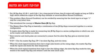
For J-Kflip-flop, if J=K=1, and if clk=1 for a long period of time, then Q output will toggle as long as CLK is
high, which makes the output of the flip-flop unstable or uncertain(Race Around Condition).
This problem (Race Around Condition) can be avoided by ensuring that the clock input is at logic “1”
only for a very short time.
This introduced the concept of Master Slave JK flip flop.
The Master-Slave Flip-Flop is basically a combination of two JK flip-flops connected together in a series
configuration.
A master-slave flip flop is made by connecting two JK flip flops in a series configuration in which one acts
as the master and another as a slave.
Here inverter and clock pulse are connected to ensure that the slave flip flop gets an inverted clock
pulse.
If CP = 0 for the master flip flop, CP=1 for slave flip flop, and vice versa.
When the clock signal transitions from low to high (also known as the rising edge), the master flip-flop
reads the inputs and stores the data temporarily.
When the clock signal transitions from high to low (the falling edge), the slave flip-flop reads the data
stored in the master flip-flop and retains it until the next clock cycle.
MASTER AND SLAVE FLIP-FLOP
43
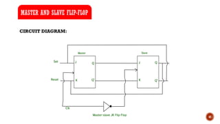
Working of amaster slave flip flop:
When the clock pulse goes to 1, the slave is isolated; J and K inputs may affect the state of
the system.The slave flip-flop is isolated until the CP goes to 0.When the CP goes back to
0, information is passed from the master flip-flop to the slave and output is obtained.
Firstly the master flip flop is positive level triggered and the slave flip flop is negative level
triggered, so the master responds before the slave.
If J=0 and K=1, the high Q’ output of the master goes to the K input of the slave and the
clock forces the slave to reset, thus the slave copies the master.
If J=1 and K=0, the high Q output of the master goes to the J input of the slave and the
Negative transition of the clock sets the slave, copying the master.
If J=1 and K=1, it toggles on the positive transition of the clock and thus the slave toggles
on the negative transition of the clock.
If J=0 and K=0, the flip flop is disabled and Q remains unchanged.
MASTER AND SLAVE FLIP-FLOP
44.
44
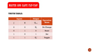
MASTER AND SLAVEFLIP-FLOP
TRUTH TABLE:
Inputs Output
Operation
Mode
J K Qn+1
0 0 Qn No Change
0 1 0 Reset
1 0 1 Set
1 1 Qn' Toggle
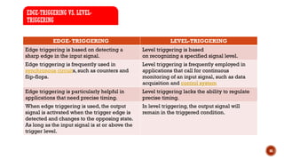
46
EDGE-TRIGGERING VS. LEVEL-
TRIGGERING
EDGE-TRIGGERING LEVEL-TRIGGERING
Edge triggering is based on detecting a
sharp edge in the input signal.
Level triggering is based
on recognizing a specified signal level.
Edge triggering is frequently used in
synchronous circuits, such as counters and
flip-flops.
Level triggering is frequently employed in
applications that call for continuous
monitoring of an input signal, such as data
acquisition and control system
Edge triggering is particularly helpful in
applications that need precise timing.
Level triggering lacks the ability to regulate
precise timing.
When edge triggering is used, the output
signal is activated when the trigger edge is
detected and changes to the opposing state.
As long as the input signal is at or above the
trigger level.
In level triggering, the output signal will
remain in the triggered condition.
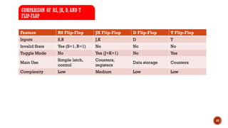
47.
47
COMPARISON OF RS,JK, D, AND T
FLIP-FLOP
Feature RS Flip-Flop JK Flip-Flop D Flip-Flop T Flip-Flop
Inputs S,R J,K D T
Invalid State Yes (S=1, R=1) No No No
Toggle Mode No Yes (J=K=1) No Yes
Main Use
Simple latch,
control
Counters,
registers
Data storage Counters
Complexity Low Medium Low Low


![SEQUENTIAL CIRCUITS [FLIP FLOPS AND LATCHES]](https://cdn.slidesharecdn.com/ss_thumbnails/sequentialcircuits-211203044039-thumbnail.jpg?width=640&height=640&fit=bounds)
![SEQUENTIAL CIRCUITS [Flip-flops and Latches]](https://cdn.slidesharecdn.com/ss_thumbnails/sequentialcircuits-211217082412-thumbnail.jpg?width=640&height=640&fit=bounds)


