Download to read offline

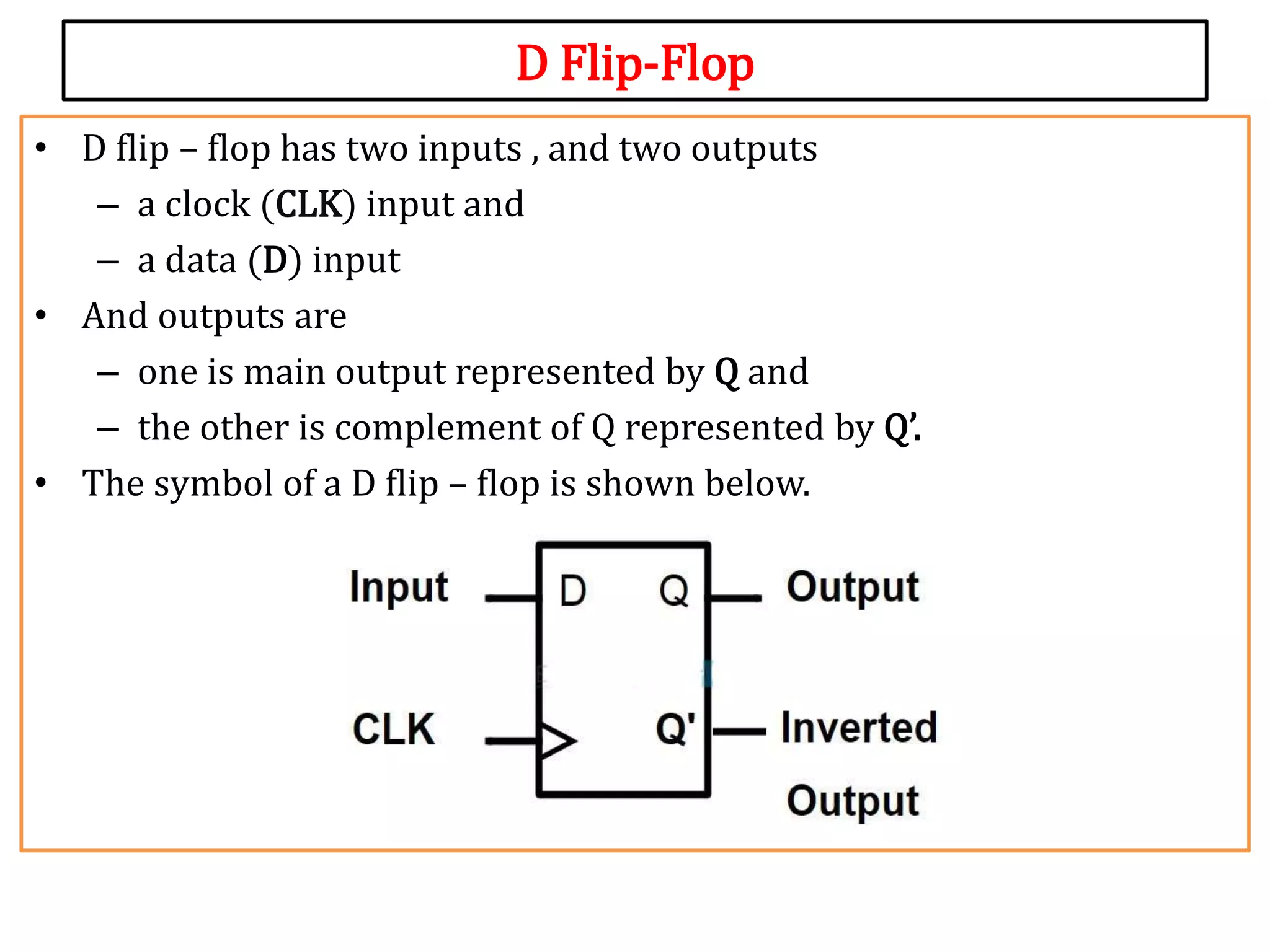
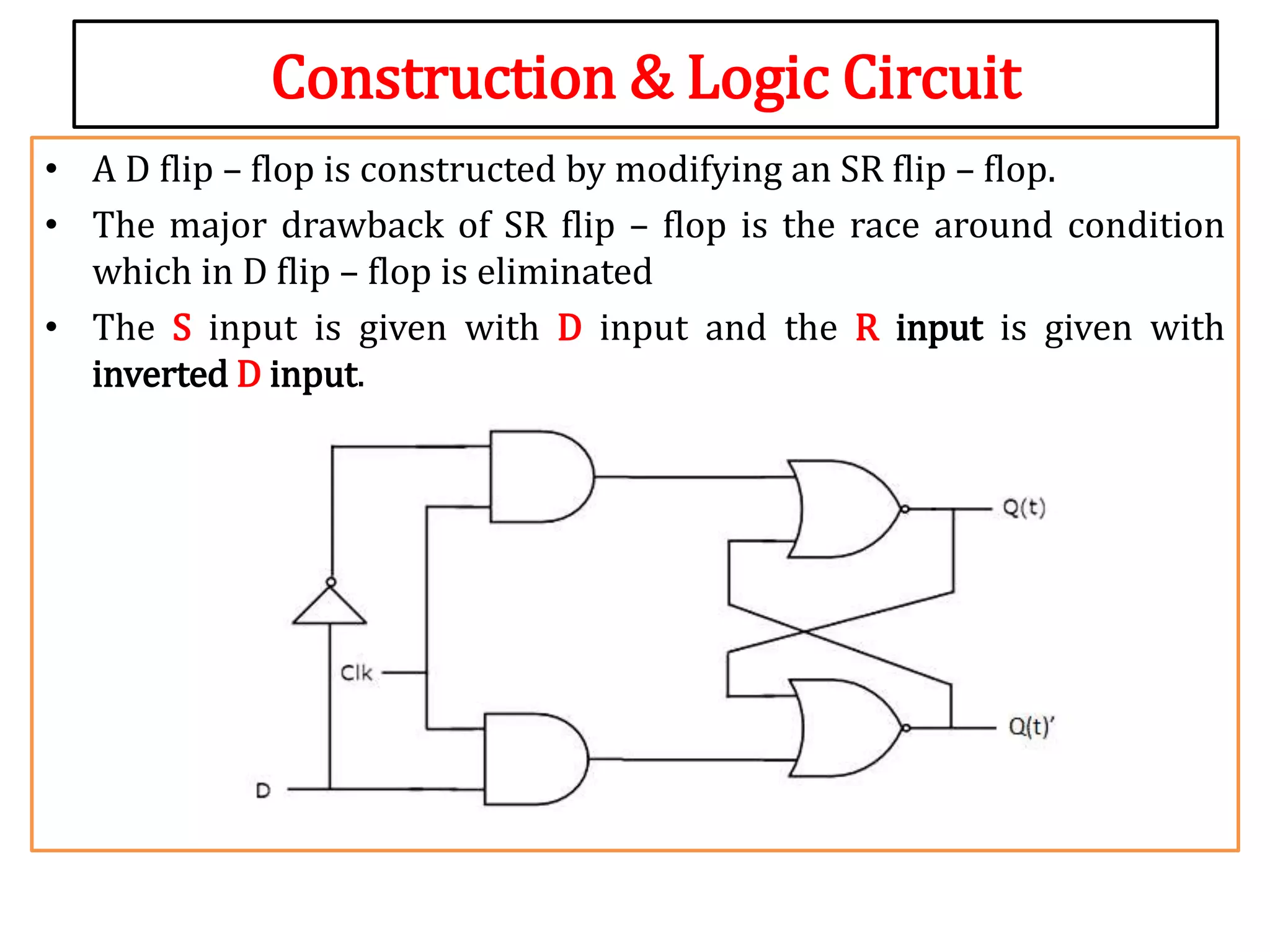
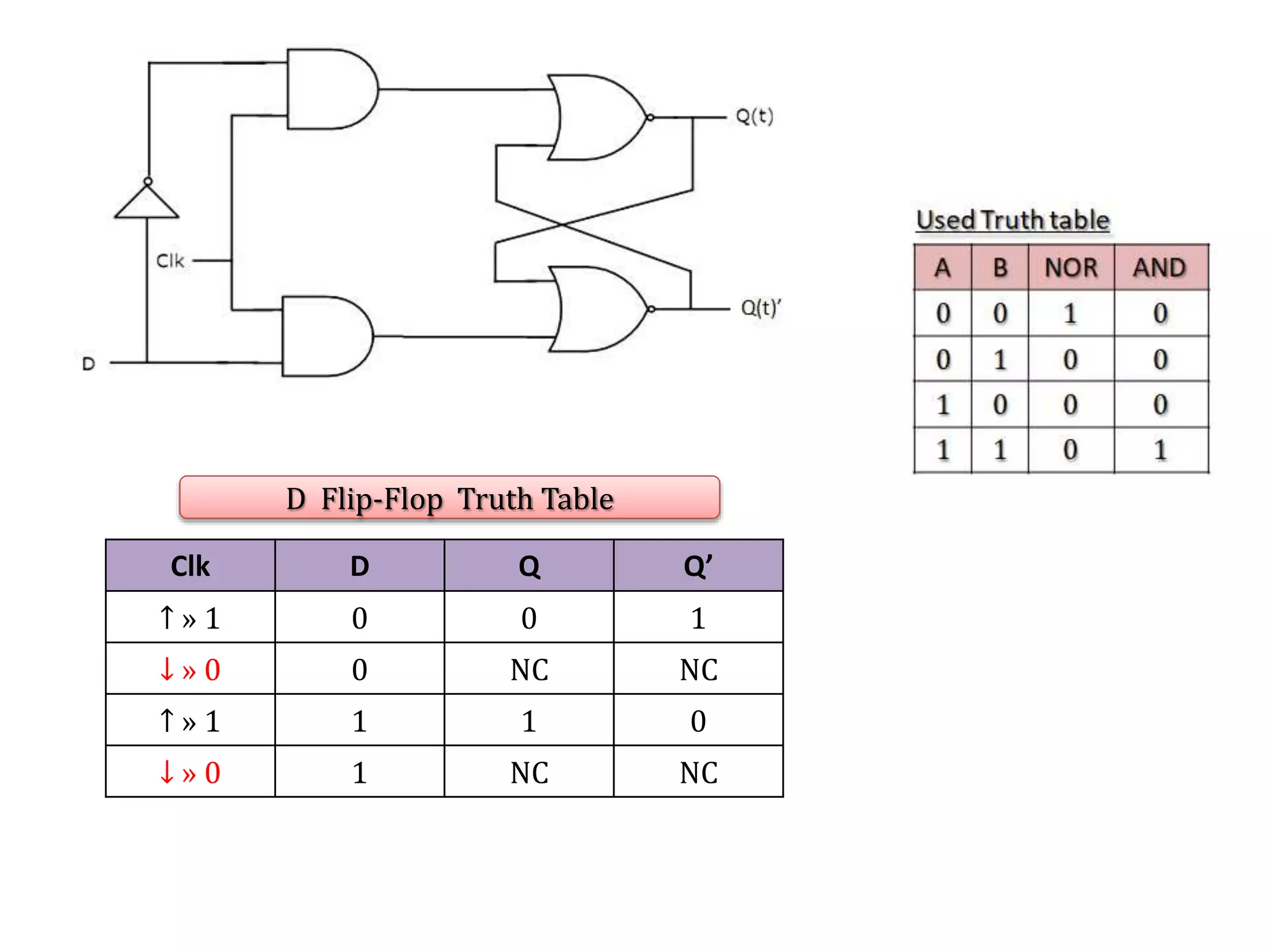
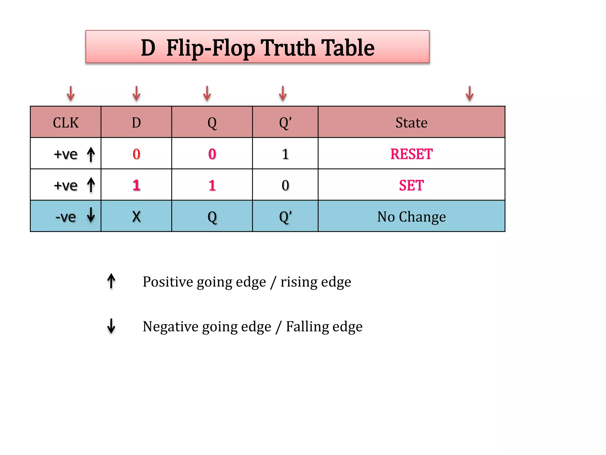
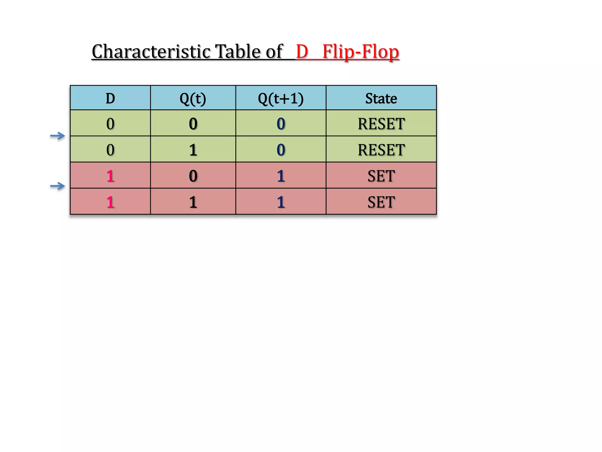
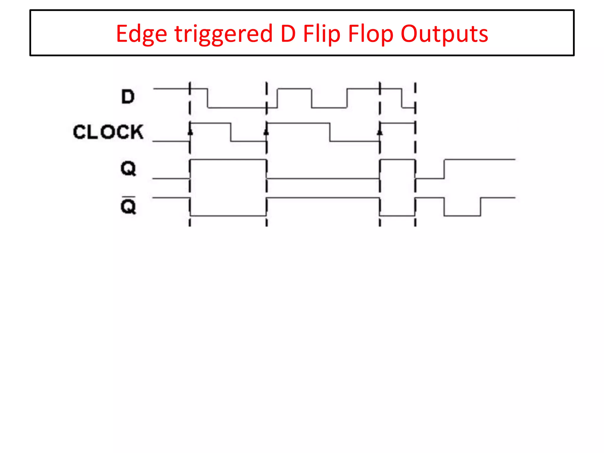


The document discusses D flip-flops, which are sequential logic circuits used to store 1-bit binary data and are popular in digital electronics. It explains their construction, how they operate using clock and data inputs, and includes their truth table and applications like data storage and shift registers. The document also notes that D flip-flops address the major drawback of SR flip-flops, specifically the race around condition.