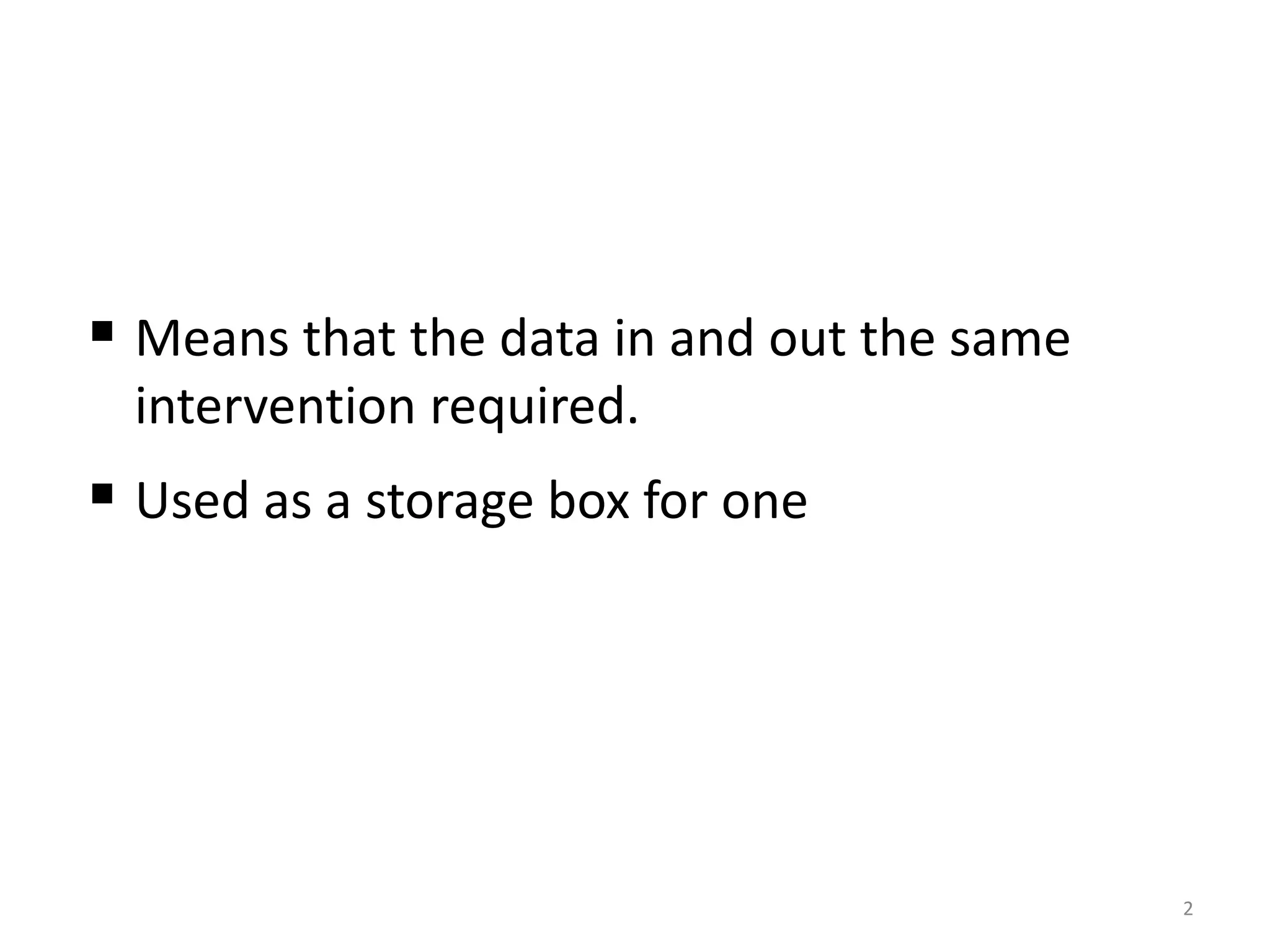
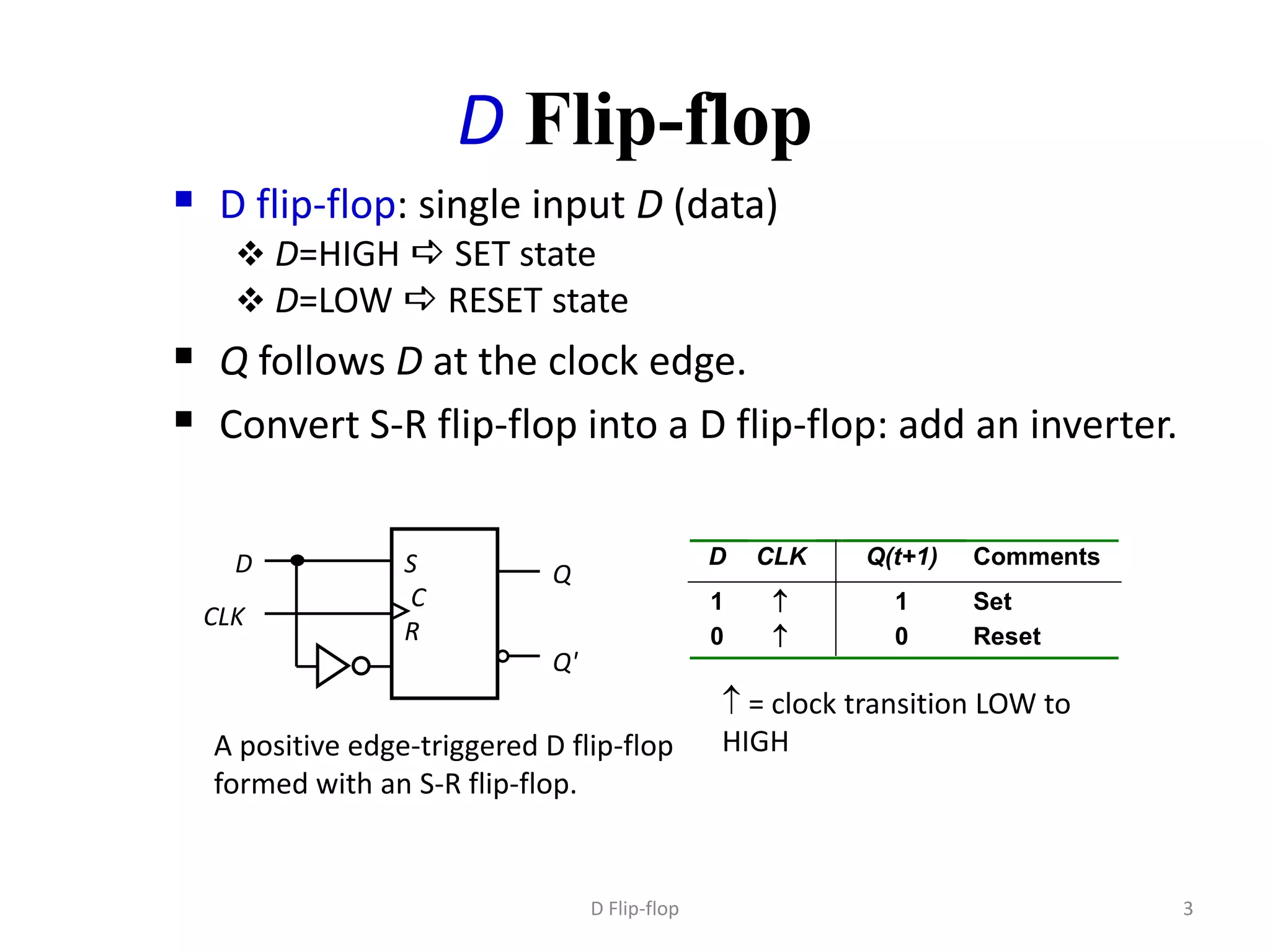
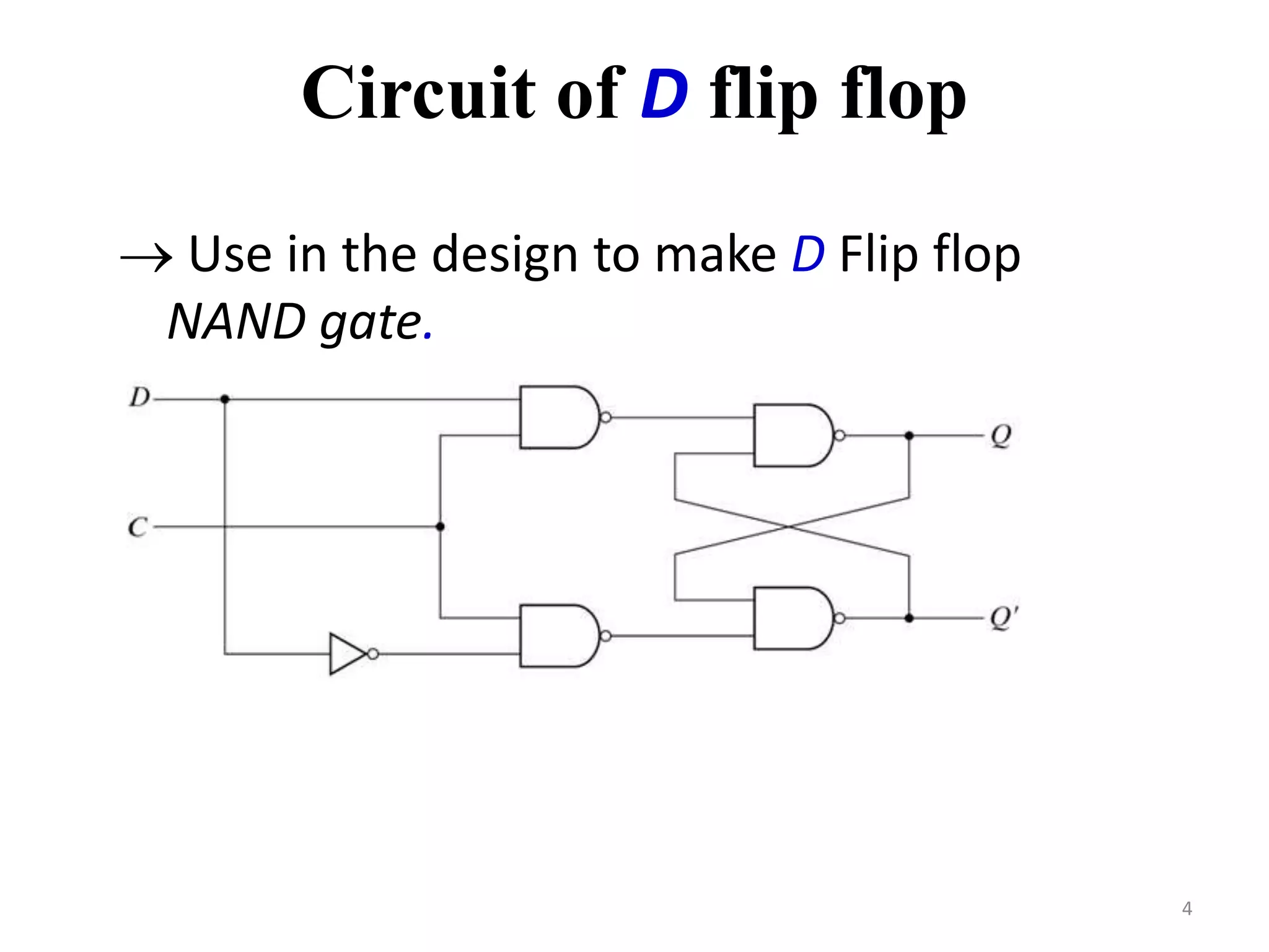
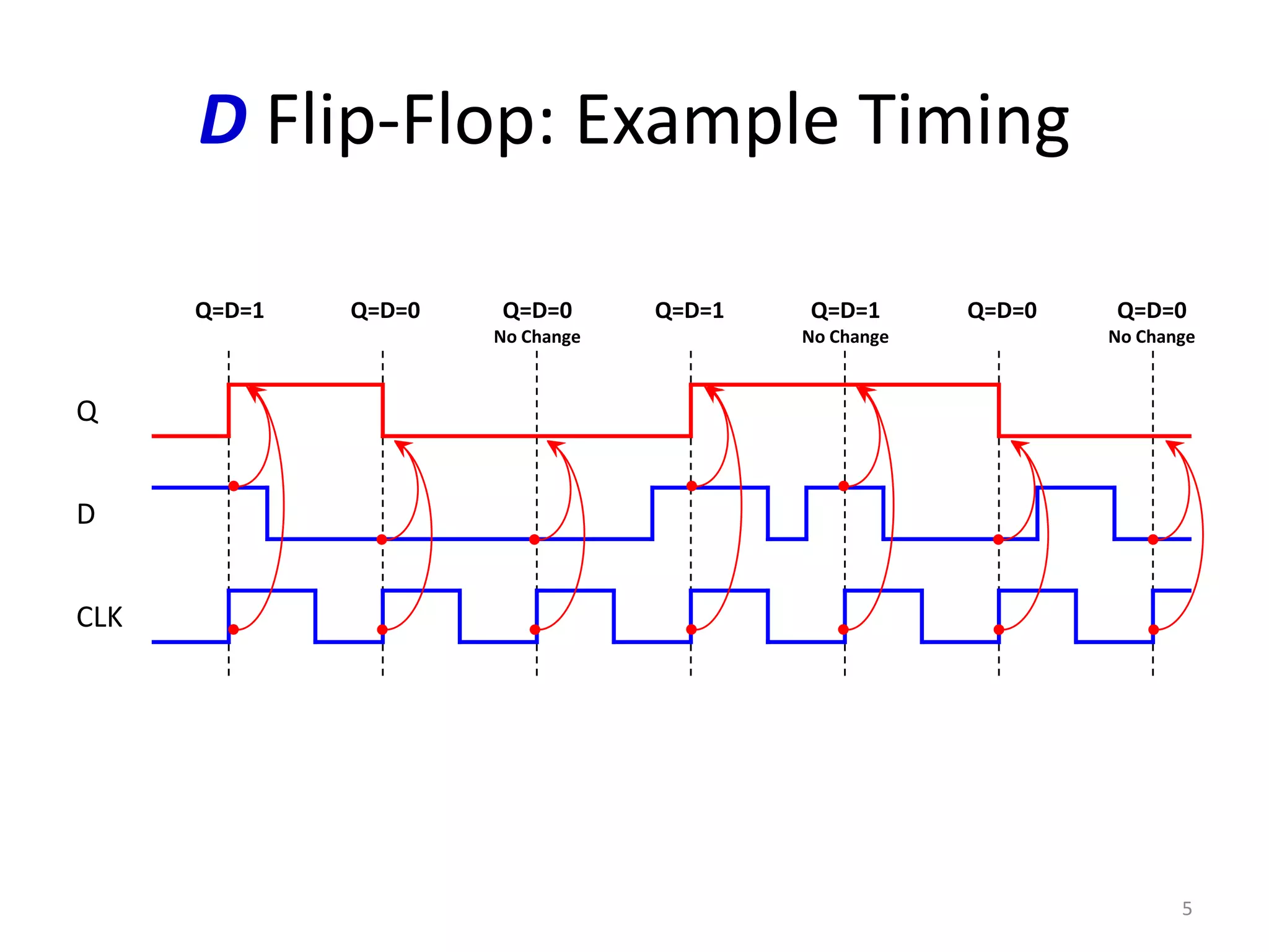
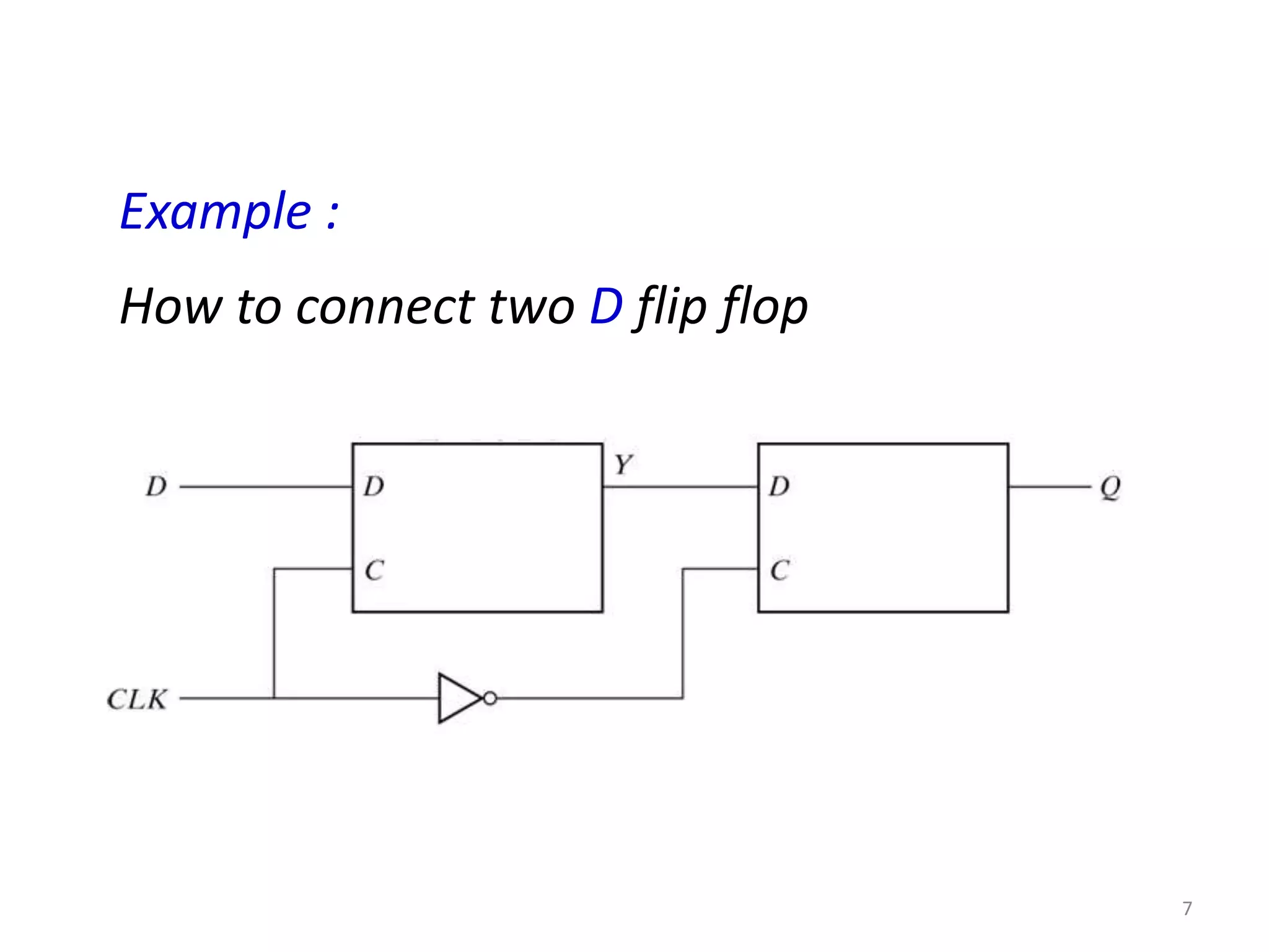
D Flip-Flop
1
2
 Means that the data in and out the same
intervention required.
 Used as a storage box for one
D Flip-flop
 D flip-flop: single input D (data)
 D=HIGH a SET state
 D=LOW a RESET state
 Q follows D at the clock edge.
 Convert S-R flip-flop into a D flip-flop: add an inverter.
D Flip-flop 3
A positive edge-triggered D flip-flop
formed with an S-R flip-flop.
S
C
R
Q
Q'
CLK
D D CLK Q(t+1) Comments
1  1 Set
0  0 Reset
 = clock transition LOW to
HIGH
 Use in the design to make D Flip flop
NAND gate.
Circuit of D flip flop
4
D Flip-Flop: Example Timing
5
Q
D
CLK
Q=D=1 Q=D=1Q=D=0 Q=D=1
No Change
Q=D=0
No Change
Q=D=0
No Change
Q=D=0
POS & NEG Edge Triggered D
6
QCLK
D Q
D CLK
0  0 1
1  1 0
 : Rising Edge of Clock
QQ
D CLK
0  0 1
1  1 0
 : Falling Edge of Clock
QQ
QCLK
D Q
Positive Edge Trigger
Negative Edge Trigger
Example :
How to connect two D flip flop
7
Ring counters are implemented using shift registers. It is essentially a
circulating shift register connected so that the last flip-flop shifts its value into
the first flip-flop. There is usually only a single 1 circulating in the register, as
long as clock pulses are applied. (Starts 1000->0100->0010->0001 repeat)
Ring Counter
8
1000
0001 0010
0100
Clock Q0 Q1 Q2 Q3
0 1 0 0 0
1 0 1 0 0
2 0 0 1 0
3 0 0 0 1
Partner work
9
Partner work
 Example: Connect )6-bit( the ring counter and complete the schedule ?
10
CLK
Q0
D Q D Q D Q D Q D Q D Q
Q1 Q2 Q3 Q4 Q5
Clock Q0 Q1 Q2 Q3 Q4 Q5
0
1
2
3
4
5
Partner work
 Example: Connect )6-bit( the ring counter and complete the schedule ?
11
CLK
Q0
D Q D Q D Q D Q D Q D Q
Q1 Q2 Q3 Q4 Q5
Clock Q0 Q1 Q2 Q3 Q4 Q5
0 1 0 0 0 0 0
1 0 1 0 0 0 0
2 0 0 1 0 0 0
3 0 0 0 1 0 0
4 0 0 0 0 1 0
5 0 0 0 0 0 1
100000
010000
001000
000100
000010
000001
Summary
12
Questions
13
Thank you for lesson

Trts d flip flop1

  • 1.
  • 2.
    2  Means thatthe data in and out the same intervention required.  Used as a storage box for one
  • 3.
    D Flip-flop  Dflip-flop: single input D (data)  D=HIGH a SET state  D=LOW a RESET state  Q follows D at the clock edge.  Convert S-R flip-flop into a D flip-flop: add an inverter. D Flip-flop 3 A positive edge-triggered D flip-flop formed with an S-R flip-flop. S C R Q Q' CLK D D CLK Q(t+1) Comments 1  1 Set 0  0 Reset  = clock transition LOW to HIGH
  • 4.
     Use inthe design to make D Flip flop NAND gate. Circuit of D flip flop 4
  • 5.
    D Flip-Flop: ExampleTiming 5 Q D CLK Q=D=1 Q=D=1Q=D=0 Q=D=1 No Change Q=D=0 No Change Q=D=0 No Change Q=D=0
  • 6.
    POS & NEGEdge Triggered D 6 QCLK D Q D CLK 0  0 1 1  1 0  : Rising Edge of Clock QQ D CLK 0  0 1 1  1 0  : Falling Edge of Clock QQ QCLK D Q Positive Edge Trigger Negative Edge Trigger
  • 7.
    Example : How toconnect two D flip flop 7
  • 8.
    Ring counters areimplemented using shift registers. It is essentially a circulating shift register connected so that the last flip-flop shifts its value into the first flip-flop. There is usually only a single 1 circulating in the register, as long as clock pulses are applied. (Starts 1000->0100->0010->0001 repeat) Ring Counter 8 1000 0001 0010 0100 Clock Q0 Q1 Q2 Q3 0 1 0 0 0 1 0 1 0 0 2 0 0 1 0 3 0 0 0 1
  • 9.
  • 10.
    Partner work  Example:Connect )6-bit( the ring counter and complete the schedule ? 10 CLK Q0 D Q D Q D Q D Q D Q D Q Q1 Q2 Q3 Q4 Q5 Clock Q0 Q1 Q2 Q3 Q4 Q5 0 1 2 3 4 5
  • 11.
    Partner work  Example:Connect )6-bit( the ring counter and complete the schedule ? 11 CLK Q0 D Q D Q D Q D Q D Q D Q Q1 Q2 Q3 Q4 Q5 Clock Q0 Q1 Q2 Q3 Q4 Q5 0 1 0 0 0 0 0 1 0 1 0 0 0 0 2 0 0 1 0 0 0 3 0 0 0 1 0 0 4 0 0 0 0 1 0 5 0 0 0 0 0 1 100000 010000 001000 000100 000010 000001
  • 12.
  • 13.

Editor's Notes

  • #6 Timing diagram example for a D flip-flop.
  • #7 Schematic symbol and excitation table for the positive edge triggered and negative edge triggered D flip-flops