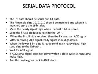
SERIAL DATA PROTOCOL

• The I/P data should be serial one bit data.
• The Preamble data 10101010 should be matched and when it is
  matched store the 16 bit data.
• Make the Ready signal High When the first 8 bit is stored.
• Send the first 8 bit data parallel to the O/ P.
• When the first 8 bit is received then the Rx sends an ACK signal.
• After receiving ACK signal ready signal should go down.
• When the lower 8 bit data is ready send again ready signal high
  send data to the O/P port.
• Wait for ACK signal.
• If ACK signal signal does not come within 7 clock cycle ERROR signal
  make high.
• And the device goes back to IDLE state.
TOP LEVEL MODULE


S_in
                 Dout parallel

                     ACK
Clock
                     Ready

         Reset
Clock signal flow graph
clk
rst

din

SHift_en


Shift_Reg

Ready
 Ack


dout
error
TOP LEVEL INTERNAL MODULE


                 Shift REGISTER SIPO
S_in                                      Dout parallel
                                          8 bit

                    TD_En         SD_En

Clock
                                               AKW
                  STATE MACHINE
                                          Ready


                     Reset
STATE MACHINE(Description)
• The state machine diagram is used to detect
  the Preamble Data.
• The Preamble data Format is 10101010.
• As it detect the Header Data it Enable the Shift
  register for next 16 bit.
• At the same time as the register is 8 bit long.
• For the Synchronization of 8 bit data to output
  there is one more counter which enable the
  TX_Data signal High as the 8 bit is stored.
STATE MACHINE(cont…)
• When the data transfer is complete it again go
  to the next state to check the Header Data
  format.
• Thus the state machine moves from one state
  to another until the next header is detected.

• Complete:
STATE MACHINE DIAGRAM
                                            reset
                                                         Din== X

                                        idle        0
                                1
                                                                            0
              TD_En=1’b1                0                   s1
count !=16
           Ready=1’b1 S8
                                                                            1
             SD_En=1’b1

                  1
                                                                   1    s2
                       0
             S7                                                                 0

             0                                              0
                           1
                  S6                                                   s3
                                    0           1                  1
                       1
                               S5                   S4
                                            0
SHIFT REGISTER
• The shift register should shift the 16 bit data.
• When the data is shifted send the 8 bit data to
  O/P.
• When the data is Received Rx should send
  ACK signal then shift register transfer its
  another 8 bit data to the output.
• The output data should be 8 bit parallel in
  nature.
SHIFT REGISTER


Sin
         Sequential
           Block      Combo
clk                    Block
                               Dout
SD_En


TD_En


             reset
TEST BENCH
• The test bench should generate the clock and
  reset signal.
• The transfer of data should go the top
  module goes serially.
• The transfer of data take place at each clock
  edge.
• On receiving the 8 bit data send the ACK
  signal.
• Test the top module.
Ethertnet data transfer.ppt

Ethertnet data transfer.ppt

  • 1.
    SERIAL DATA PROTOCOL •The I/P data should be serial one bit data. • The Preamble data 10101010 should be matched and when it is matched store the 16 bit data. • Make the Ready signal High When the first 8 bit is stored. • Send the first 8 bit data parallel to the O/ P. • When the first 8 bit is received then the Rx sends an ACK signal. • After receiving ACK signal ready signal should go down. • When the lower 8 bit data is ready send again ready signal high send data to the O/P port. • Wait for ACK signal. • If ACK signal signal does not come within 7 clock cycle ERROR signal make high. • And the device goes back to IDLE state.
  • 2.
    TOP LEVEL MODULE S_in Dout parallel ACK Clock Ready Reset
  • 3.
    Clock signal flowgraph clk rst din SHift_en Shift_Reg Ready Ack dout error
  • 4.
    TOP LEVEL INTERNALMODULE Shift REGISTER SIPO S_in Dout parallel 8 bit TD_En SD_En Clock AKW STATE MACHINE Ready Reset
  • 5.
    STATE MACHINE(Description) • Thestate machine diagram is used to detect the Preamble Data. • The Preamble data Format is 10101010. • As it detect the Header Data it Enable the Shift register for next 16 bit. • At the same time as the register is 8 bit long. • For the Synchronization of 8 bit data to output there is one more counter which enable the TX_Data signal High as the 8 bit is stored.
  • 6.
    STATE MACHINE(cont…) • Whenthe data transfer is complete it again go to the next state to check the Header Data format. • Thus the state machine moves from one state to another until the next header is detected. • Complete:
  • 7.
    STATE MACHINE DIAGRAM reset Din== X idle 0 1 0 TD_En=1’b1 0 s1 count !=16 Ready=1’b1 S8 1 SD_En=1’b1 1 1 s2 0 S7 0 0 0 1 S6 s3 0 1 1 1 S5 S4 0
  • 8.
    SHIFT REGISTER • Theshift register should shift the 16 bit data. • When the data is shifted send the 8 bit data to O/P. • When the data is Received Rx should send ACK signal then shift register transfer its another 8 bit data to the output. • The output data should be 8 bit parallel in nature.
  • 9.
    SHIFT REGISTER Sin Sequential Block Combo clk Block Dout SD_En TD_En reset
  • 10.
    TEST BENCH • Thetest bench should generate the clock and reset signal. • The transfer of data should go the top module goes serially. • The transfer of data take place at each clock edge. • On receiving the 8 bit data send the ACK signal. • Test the top module.