Downloaded 221 times


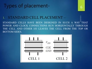


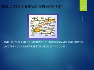
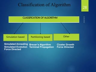

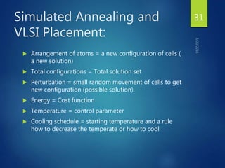

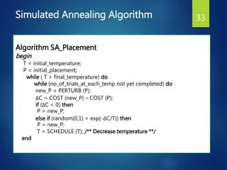
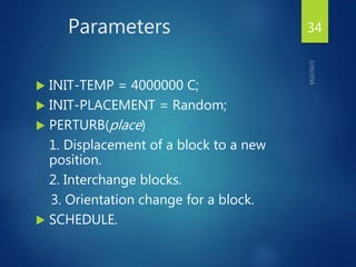


Placement is the process of determining the locations of circuit devices on a chip. It is a critical step that affects performance, routability, heat distribution, and power consumption. There are different types of placement like standard cell placement and building block placement. Placement algorithms aim to optimize objectives like minimizing total area and wire length. Simulated annealing is a commonly used iterative placement algorithm that models the physical annealing process to arrive at a low-cost solution. Other algorithms include partitioning-based approaches and cluster growth.


