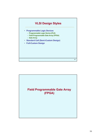
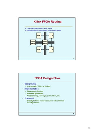
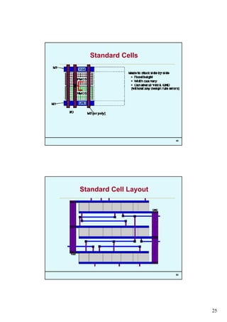
This document discusses various VLSI design styles including programmable logic devices (PLDs), field programmable gate arrays (FPGAs), gate arrays, standard cells, and full-custom design. FPGAs use an array of logic cells connected by routing channels with configurable interconnects implemented using SRAM switches. Gate arrays have a two-step manufacturing process where generic masks are first used to create transistor arrays that are later customized using metal interconnect masks. Standard cell design uses pre-designed and characterized logic cells stored in a library that can be placed in rows with power and ground rails for semi-custom designs. Full-custom design involves creating new mask designs without libraries for the entire chip layout.
