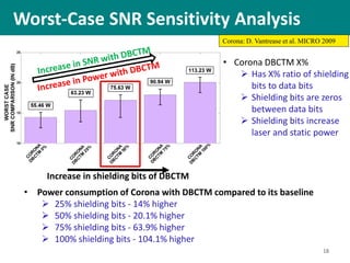
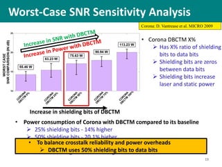
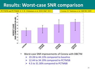
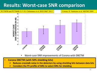
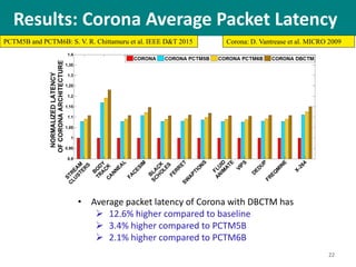
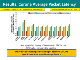
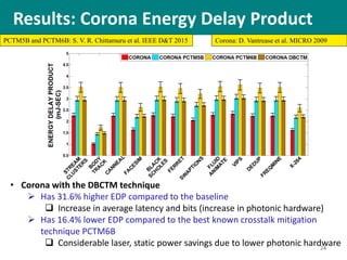
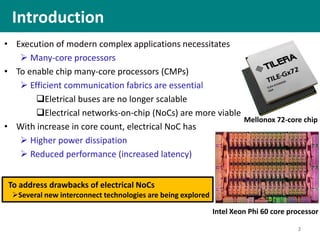
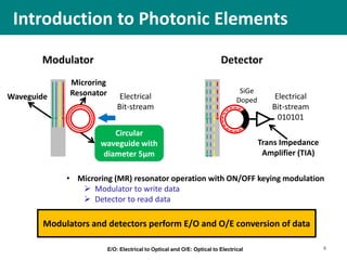
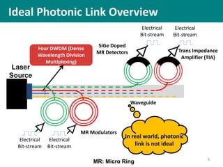
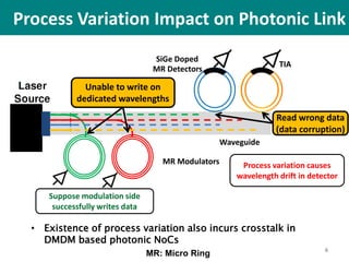
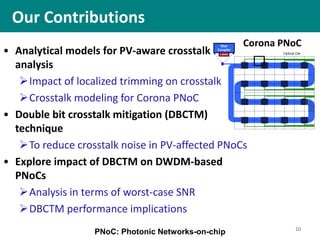
MWSCAS 2015
Fort Collins, Colorado, USA
August 2-5, 2015
Process Variation Aware Crosstalk Mitigation
for DWDM based Photonic NoC Architectures
Sai Vineel Reddy Chittamuru, Ishan Thakkar and Sudeep Pasricha
Department of Electrical and Computer Engineering
Colorado State University, Fort Collins, CO, U.S.A.
{sai.chittamuru, ishan.thakkar, sudeep}@colostate.edu
DOI: 10.1109/ISQED.2016.7479176
• Introduction
• Motivation and Contributions
• Related Work
• Impact of Localized Trimming on Crosstalk
• Double-bit Crosstalk Mitigation Technique
• Experimental Results
• Conclusion
Outline
1
Introduction
• Execution of modern complex applications necessitates
 Many-core processors
• To enable chip many-core processors (CMPs)
 Efficient communication fabrics are essential
Eletrical buses are no longer scalable
Electrical networks-on-chip (NoCs) are more viable
• With increase in core count, electrical NoC has
 Higher power dissipation
 Reduced performance (increased latency)
2
Mellonox 72-core chip
Intel Xeon Phi 60 core processor
To address drawbacks of electrical NoCs
Several new interconnect technologies are being explored
Benefits of Photonic Interconnects
3Source: L. Xu, et al. IEEE-PTL, 2012 and S. V. R. Chittamuru, et al. GLSVLSI 2015
• Photonic interconnects are potential solution to address
drawbacks of copper wire based electrical interconnects
• Advantages of photonic interconnects over copper wires:
 High bandwidth (~40 Gbps) with DWDM (dense
wavelength division multiplexing)
5× or higher compared to copper wires
 Low latency (10.45 ps/mm)
10× faster than copper wires
 Low power (7.9 fJ/bit)
 Better scalability, no pin limits
Photonic links for data communicationNoCs that use photonic interconnects provide higher
bandwidth with lower power consumption
Microring Resonator
4
Introduction to Photonic Elements
Modulator Detector
Electrical
Bit-stream
Electrical
Bit-stream
010101
Modulators and detectors perform E/O and O/E conversion of data
• Microring (MR) resonator operation with ON/OFF keying modulation
 Modulator to write data
 Detector to read data
SiGe
DopedWaveguide
Microring
Resonator
Circular
waveguide with
diameter 5µm
Trans Impedance
Amplifier (TIA)
E/O: Electrical to Optical and O/E: Optical to Electrical
101010010101010010100
Ideal Photonic Link Overview
5
Electrical
Bit-stream
Electrical
Bit-stream
Electrical
Bit-stream
Electrical
Bit-stream
MR Modulators
SiGe Doped
MR Detectors Trans Impedance
Amplifier (TIA)
Waveguide
Four DWDM (Dense
Wavelength Division
Multiplexing)
In real world, photonic
link is not ideal
MR: Micro Ring
6
• Existence of process variation also incurs crosstalk in
DMDM based photonic NoCs
MR Modulators
MR Detectors
SiGe Doped
TIA
Waveguide
Process variation causes
resonance wavelength drift
Unable to write on
dedicated wavelengths
Suppose modulation side
successfully writes data
Process variation causes
wavelength drift in detector
Read wrong data
(data corruption)
Process Variation Impact on Photonic Link
MR: Micro Ring
PV-Induced Crosstalk in Photonic Link
7
Electrical
Bit-stream
Electrical
Bit-stream
MR modulators
SiGe doped
MR detectors
Trans Impedance
Amplifier (TIA)
Waveguide
Crosstalk noise in
detector
Crosstalk noise
in waveguide
Electrical bit-streams with noise
• PV-induced crosstalk noise in ring detectors
 Decreases Signal to Noise Ratio (SNR)
 Increases Bit Error Rate (BER)
 Threatens reliable photonic communication
Crosstalk noise
in modulator
MR: Micro Ring
PV-Induced Crosstalk in Photonic Link
8
Electrical
Bit-stream
Electrical
Bit-stream
MR modulators
SiGe doped
MR detectors
Trans Impedance
Amplifier (TIA)
Waveguide
Crosstalk noise in
detector
Crosstalk noise
in waveguide
Electrical bit-streams with noise
• PV-induced crosstalk noise in ring detectors
 Decreases Signal to Noise Ratio (SNR)
 Increases Bit Error Rate (BER)
 Threatens reliable photonic communicationPV-induced crosstalk noise in MR detector needs to be mitigated
for reliable photonic communication
Crosstalk noise
in modulator
MR: Micro Ring
9
Voltage Tuning (Trimming):
=VON
VR
Input Port Output Port
n+
p+ n+
Thermal Tuning:
Input Port Output Port
Micro Heater
Wavelength
PowerTransmission
Voltage Tuning
Blue Shift
Wavelength
PowerTransmission
Thermal Tuning
Red Shift
These solutions increase intrinsic optical loss and crosstalk noise in
MRs and motivate new crosstalk mitigation mechanisms
How to Tolerate Process Variations?
Our Contributions
10
• Analytical models for PV-aware crosstalk
analysis
Impact of localized trimming on crosstalk
Crosstalk modeling for Corona PNoC
• Double bit crosstalk mitigation (DBCTM)
technique
To reduce crosstalk noise in PV-affected PNoCs
• Explore impact of DBCTM on DWDM-based
PNoCs
Analysis in terms of worst-case SNR
DBCTM performance implications
PNoC: Photonic Networks-on-chip
Corona PNoC
• Introduction
• Motivation and Contributions
• Related Work
• Impact of Localized Trimming on Crosstalk
• Double-bit Crosstalk Mitigation Technique
• Experimental Results
• Conclusion
Outline
11
Device Level Crosstalk:
• [C. H. Chen WOCC 2012] Crosstalk noise in single waveguide crossings is
shown to be close to -47.58 dB
• [Q. Xu, et al. Opt. Exp. 2006] A cascaded MR-based modulator is proposed
for low-density DWDM waveguides, with an extinction ratio of 13dB
• These works show that crosstalk noise is negligible at device level
Network Level Crosstalk and Mitigation:
• [L.H.K. Duong, et al. IEEE D&T 2014] Crosstalk analysis for the Corona
PNoC, where its data channels are studied and worst-case SNR is
estimated to be 14dB
• [S. V. R. Chittamuru, et al. IEEE D&T 2015] two encoding techniques
PCTM5B and PCTM6B are presented to mitigate the impacts of
crosstalk noise in DWDM based PNoCs.
• These works do not consider process variations and their impact on
crosstalk
Related Work
12
None of these works consider PV-aware crosstalk mitigation
Impact of Localized Trimming on Crosstalk
13
𝜱 𝒊, 𝒋 =
𝜹 𝟐
(𝒊 − 𝐣)
𝑭𝑺𝑹
𝒏
𝟐
+ 𝜹 𝟐
𝑯𝒆𝒓𝒆 𝜹 =
𝝀𝒋
𝟐𝑸′
𝝺 𝑛𝝺 𝑛+1 𝝺 𝑛−1
TRANSMISSION
1
0
Ideal condition of MR passbands (without PV)
Increase in resonance wavelength
• We model passband overlap
with coupling factor (𝚽)
• With PV, passband shifts due
to change in refractive index
• Suppose PV induces red shift
• Trimming is used to
compensate this resonance
drift
• Passband overlap increases
with trimming of MRs
Passband overlap region
𝝺 𝑛𝝺 𝑛+1 𝝺 𝑛−1
TRANSMISSION
1
0
MR passbands with PV
Increase in resonance wavelength
Red Shift
𝝺 𝑛𝝺 𝑛+1 𝝺 𝑛−1
TRANSMISSION
1
0
MR passbands with PV after trimming
Increase in resonance wavelength
Increase in passband overlap region
Coupling factor increases with trimming of MRs
• With localized trimming
 Q-factor (Q’) of MR decreases
 Coupling factor (𝚽) and crosstalk noise increases
Impact of Localized Trimming on Crosstalk
14
Our work decreases crosstalk noise and improves
SNR in DWDM based PNoCs
0
2000
4000
6000
8000
10000
0
5
10
15
20
25
0 0.2 0.4 0.6 0.8 1
Q-factor
Increaseincouplingfactor
(φ)
Compensated PV-induced resonance shift (in nm)
increase in coupling factor
Q-factor
Double-Bit Crosstalk Mitigation Technique
15
• Crosstalk noise in PNoCs increases with
 Coupling factor (𝚽)
 Signal strength of adjacent non-resonant
wavelengths
• Localized trimming increases 𝚽
• DBCTM reduces crosstalk noise
 Modulates zero on alternate wavelengths
 Modulated zeros are shield bits
 Reduces signal strength of adjacent
non-resonant wavelengths
• Resonance shift has linear dependency on
length and width variation
Divide MRs in each
detecting node into
groups of 8 MRs
Determine the
thickness and width
variation in each MR
using SE and CD-SEM
Determine maximum
PV-induced resonance
red shifts (Δ𝛌max) in
each MR Group
Yes
Enable DBCTM
encoding in this
MR Group
Disable DBCTM
encoding in this
MR Group
No
Δ𝝺max> Δ𝝺th
DBCTM Technique
• We analyzed our DBCTM technique by porting it to Corona PNoC
 [D. Vantrease et al. MICRO 2009] Corona architecture with token slot
arbitration and 64×64 multiple write single read (MWSR) crossbar
• CMP configuration for implementation for Corona PNoC
Experimental Setup
16
Chip Many Core Configuration
Number of cores 256
Technology node 22nm
Memory controllers 32
Main memory 32GB; DDR4@30ns
Per Core:
L1 I-Cache size/Associativity 16KB/Direct Mapped Cache
L1 D-Cache size/Associativity 16KB/Direct Mapped Cache
L2 Cache size/ Associativity 128KB/ Direct Mapped Cache
L2 Coherence MOESI
Frequency 5 GHz
Issue Policy In-order
• Built a cycle accurate photonic network simulator in SystemC
• Trace driven simulations using GEM5 simulator (PARSEC benchmarks)
• 12 multithreaded application workloads from PARSEC benchmark
• Model and estimate PV in MRs using the VARIUS tool
• 100 process variation maps are considered for our evaluation
• Performance modeling using DSENT, CACTI 6.5, and circuit-level analysis
• Static and dynamic power/energy for photonic devices:
Source: [P. Grani, et al. JETC 2014] and [L.H.K. Duong, et al. IEEE Design and Test, 2014]
17
Energy consumption type Energy
Edynamic 0.42 pJ/bit
Elogic−dyn 0.18 pJ/bit
Photonic loss type Loss (in dB)
Propagation loss -0.274 per cm
Bending loss -0.005 per 90o
Inactive modulator through loss -0.0005
Active modulator power loss -0.6
Passing detector through loss -0.0005
Detecting detector power loss -1.6
Active modulator crosstalk coefficient -16
Detecting detector crosstalk coefficient -16
Performance and Energy Models
18
Worst-Case SNR Sensitivity Analysis
• Corona DBCTM X%
 Has X% ratio of shielding
bits to data bits
 Shielding bits are zeros
between data bits
 Shielding bits increase
laser and static power
• In Corona DBCTM X%
 Increase in shielding bits to data bits ratio
 reduces crosstalk noise
 Increases SNR
 Increases power consumption
• Worst SNR of Corona with DBCTM compared to its baseline
 25% shielding bits - 8.1% higher
 50% shielding bits – 19.67% higher
 75% shielding bits - 26% higher
 100% shielding bits – 40.5% higher
Corona: D. Vantrease et al. MICRO 2009
Increase in shielding bits of DBCTM
• Power consumption of Corona with DBCTM compared to its baseline
 25% shielding bits - 14% higher
 50% shielding bits - 20.1% higher
 75% shielding bits - 63.9% higher
 100% shielding bits - 104.1% higher
19
Worst-Case SNR Sensitivity Analysis
• Corona DBCTM X%
 Has X% ratio of shielding
bits to data bits
 Shielding bits are zeros
between data bits
 Shielding bits increase
laser and static power
• In Corona DBCTM X%
 Increase in shielding bits to data bits ratio
 reduces crosstalk noise
 Increases SNR
 Increases power consumption
• Worst SNR of Corona with DBCTM compared to its baseline
 25% shielding bits - 8.1% higher
 50% shielding bits – 19.67% higher
 75% shielding bits - 26% higher
 100% shielding bits – 40.5% higher
Corona: D. Vantrease et al. MICRO 2009
Increase in shielding bits of DBCTM
• Power consumption of Corona with DBCTM compared to its baseline
 25% shielding bits - 14% higher
 50% shielding bits - 20.1% higher
 75% shielding bits - 63.9% higher
 100% shielding bits - 104.1% higher
• To balance crosstalk reliability and power overheads
 DBCTM uses 50% shielding bits to data bits
20
• Worst-case SNR improvements of Corona with DBCTM
 19.28 to 44.13% compared to baseline
 12.44 to 34.19% compared to PCTM5B
 4.5 to 31.30% compared to PCTM6B
Corona: D. Vantrease et al. MICRO 2009PCTM5B and PCTM6B: S. V. R. Chittamuru et al. IEEE D&T 2015
Results: Worst-case SNR comparison
21
• Worst-case SNR improvements of Corona with DBCTM
 19.28 to 44.13% compared to baseline
 12.44 to 34.19% compared to PCTM5B
 4.5 to 31.30% compared to PCTM6B
• Corona DBCTM (with 50% shielding bits)
 Reduces crosstalk noise in the detectors by using shielding bits between data bits
 Considers the PV profile of MRs to select MRs for shielding
Corona: D. Vantrease et al. MICRO 2009PCTM5B and PCTM6B: S. V. R. Chittamuru et al. IEEE D&T 2015
Results: Worst-case SNR comparison
22
• Average packet latency of Corona with DBCTM has
 12.6% higher compared to baseline
 3.4% higher compared to PCTM5B
 2.1% higher compared to PCTM6B
Corona: D. Vantrease et al. MICRO 2009PCTM5B and PCTM6B: S. V. R. Chittamuru et al. IEEE D&T 2015
Results: Corona Average Packet Latency
23
• Average packet latency of Corona with DBCTM has
 12.6% higher compared to baseline
 3.4% higher compared to PCTM5B
 2.1% higher compared to PCTM6B
Delay due to encoding and decoding of data with DBCTM
contributes to increase in average latency
Corona: D. Vantrease et al. MICRO 2009PCTM5B and PCTM6B: S. V. R. Chittamuru et al. IEEE D&T 2015
Results: Corona Average Packet Latency
24
Corona: D. Vantrease et al. MICRO 2009
• Corona with the DBCTM technique
 Has 31.6% higher EDP compared to the baseline
 Increase in average latency and bits (increase in photonic hardware)
 Has 16.4% lower EDP compared to the best known crosstalk mitigation
technique PCTM6B
 Considerable laser, static power savings due to lower photonic hardware
PCTM5B and PCTM6B: S. V. R. Chittamuru et al. IEEE D&T 2015
Results: Corona Energy Delay Product
• Our proposed DBCTM technique with Corona PNoC
Reduces crosstalk noise in its detectors
Improves SNR by up to 44.13% compared to baseline
• Our proposed DBCTM technique compared to the best known
prior work
 Improves SNR by up to 31.30%
 Reduces EDP by 16.4%
• DBCTM technique is effective in overcoming trimming-induced
crosstalk in PNoCs to improve reliability
25
Conclusions
• Questions / Comments ?
Thank You
26

Process Variation Aware Crosstalk Mitigation for DWDM based Photonic NoC Architectures

  • 1.
    MWSCAS 2015 Fort Collins,Colorado, USA August 2-5, 2015 Process Variation Aware Crosstalk Mitigation for DWDM based Photonic NoC Architectures Sai Vineel Reddy Chittamuru, Ishan Thakkar and Sudeep Pasricha Department of Electrical and Computer Engineering Colorado State University, Fort Collins, CO, U.S.A. {sai.chittamuru, ishan.thakkar, sudeep}@colostate.edu DOI: 10.1109/ISQED.2016.7479176
  • 2.
    • Introduction • Motivationand Contributions • Related Work • Impact of Localized Trimming on Crosstalk • Double-bit Crosstalk Mitigation Technique • Experimental Results • Conclusion Outline 1
  • 3.
    Introduction • Execution ofmodern complex applications necessitates  Many-core processors • To enable chip many-core processors (CMPs)  Efficient communication fabrics are essential Eletrical buses are no longer scalable Electrical networks-on-chip (NoCs) are more viable • With increase in core count, electrical NoC has  Higher power dissipation  Reduced performance (increased latency) 2 Mellonox 72-core chip Intel Xeon Phi 60 core processor To address drawbacks of electrical NoCs Several new interconnect technologies are being explored
  • 4.
    Benefits of PhotonicInterconnects 3Source: L. Xu, et al. IEEE-PTL, 2012 and S. V. R. Chittamuru, et al. GLSVLSI 2015 • Photonic interconnects are potential solution to address drawbacks of copper wire based electrical interconnects • Advantages of photonic interconnects over copper wires:  High bandwidth (~40 Gbps) with DWDM (dense wavelength division multiplexing) 5× or higher compared to copper wires  Low latency (10.45 ps/mm) 10× faster than copper wires  Low power (7.9 fJ/bit)  Better scalability, no pin limits Photonic links for data communicationNoCs that use photonic interconnects provide higher bandwidth with lower power consumption Microring Resonator
  • 5.
    4 Introduction to PhotonicElements Modulator Detector Electrical Bit-stream Electrical Bit-stream 010101 Modulators and detectors perform E/O and O/E conversion of data • Microring (MR) resonator operation with ON/OFF keying modulation  Modulator to write data  Detector to read data SiGe DopedWaveguide Microring Resonator Circular waveguide with diameter 5µm Trans Impedance Amplifier (TIA) E/O: Electrical to Optical and O/E: Optical to Electrical 101010010101010010100
  • 6.
    Ideal Photonic LinkOverview 5 Electrical Bit-stream Electrical Bit-stream Electrical Bit-stream Electrical Bit-stream MR Modulators SiGe Doped MR Detectors Trans Impedance Amplifier (TIA) Waveguide Four DWDM (Dense Wavelength Division Multiplexing) In real world, photonic link is not ideal MR: Micro Ring
  • 7.
    6 • Existence ofprocess variation also incurs crosstalk in DMDM based photonic NoCs MR Modulators MR Detectors SiGe Doped TIA Waveguide Process variation causes resonance wavelength drift Unable to write on dedicated wavelengths Suppose modulation side successfully writes data Process variation causes wavelength drift in detector Read wrong data (data corruption) Process Variation Impact on Photonic Link MR: Micro Ring
  • 8.
    PV-Induced Crosstalk inPhotonic Link 7 Electrical Bit-stream Electrical Bit-stream MR modulators SiGe doped MR detectors Trans Impedance Amplifier (TIA) Waveguide Crosstalk noise in detector Crosstalk noise in waveguide Electrical bit-streams with noise • PV-induced crosstalk noise in ring detectors  Decreases Signal to Noise Ratio (SNR)  Increases Bit Error Rate (BER)  Threatens reliable photonic communication Crosstalk noise in modulator MR: Micro Ring
  • 9.
    PV-Induced Crosstalk inPhotonic Link 8 Electrical Bit-stream Electrical Bit-stream MR modulators SiGe doped MR detectors Trans Impedance Amplifier (TIA) Waveguide Crosstalk noise in detector Crosstalk noise in waveguide Electrical bit-streams with noise • PV-induced crosstalk noise in ring detectors  Decreases Signal to Noise Ratio (SNR)  Increases Bit Error Rate (BER)  Threatens reliable photonic communicationPV-induced crosstalk noise in MR detector needs to be mitigated for reliable photonic communication Crosstalk noise in modulator MR: Micro Ring
  • 10.
    9 Voltage Tuning (Trimming): =VON VR InputPort Output Port n+ p+ n+ Thermal Tuning: Input Port Output Port Micro Heater Wavelength PowerTransmission Voltage Tuning Blue Shift Wavelength PowerTransmission Thermal Tuning Red Shift These solutions increase intrinsic optical loss and crosstalk noise in MRs and motivate new crosstalk mitigation mechanisms How to Tolerate Process Variations?
  • 11.
    Our Contributions 10 • Analyticalmodels for PV-aware crosstalk analysis Impact of localized trimming on crosstalk Crosstalk modeling for Corona PNoC • Double bit crosstalk mitigation (DBCTM) technique To reduce crosstalk noise in PV-affected PNoCs • Explore impact of DBCTM on DWDM-based PNoCs Analysis in terms of worst-case SNR DBCTM performance implications PNoC: Photonic Networks-on-chip Corona PNoC
  • 12.
    • Introduction • Motivationand Contributions • Related Work • Impact of Localized Trimming on Crosstalk • Double-bit Crosstalk Mitigation Technique • Experimental Results • Conclusion Outline 11
  • 13.
    Device Level Crosstalk: •[C. H. Chen WOCC 2012] Crosstalk noise in single waveguide crossings is shown to be close to -47.58 dB • [Q. Xu, et al. Opt. Exp. 2006] A cascaded MR-based modulator is proposed for low-density DWDM waveguides, with an extinction ratio of 13dB • These works show that crosstalk noise is negligible at device level Network Level Crosstalk and Mitigation: • [L.H.K. Duong, et al. IEEE D&T 2014] Crosstalk analysis for the Corona PNoC, where its data channels are studied and worst-case SNR is estimated to be 14dB • [S. V. R. Chittamuru, et al. IEEE D&T 2015] two encoding techniques PCTM5B and PCTM6B are presented to mitigate the impacts of crosstalk noise in DWDM based PNoCs. • These works do not consider process variations and their impact on crosstalk Related Work 12 None of these works consider PV-aware crosstalk mitigation
  • 14.
    Impact of LocalizedTrimming on Crosstalk 13 𝜱 𝒊, 𝒋 = 𝜹 𝟐 (𝒊 − 𝐣) 𝑭𝑺𝑹 𝒏 𝟐 + 𝜹 𝟐 𝑯𝒆𝒓𝒆 𝜹 = 𝝀𝒋 𝟐𝑸′ 𝝺 𝑛𝝺 𝑛+1 𝝺 𝑛−1 TRANSMISSION 1 0 Ideal condition of MR passbands (without PV) Increase in resonance wavelength • We model passband overlap with coupling factor (𝚽) • With PV, passband shifts due to change in refractive index • Suppose PV induces red shift • Trimming is used to compensate this resonance drift • Passband overlap increases with trimming of MRs Passband overlap region 𝝺 𝑛𝝺 𝑛+1 𝝺 𝑛−1 TRANSMISSION 1 0 MR passbands with PV Increase in resonance wavelength Red Shift 𝝺 𝑛𝝺 𝑛+1 𝝺 𝑛−1 TRANSMISSION 1 0 MR passbands with PV after trimming Increase in resonance wavelength Increase in passband overlap region Coupling factor increases with trimming of MRs
  • 15.
    • With localizedtrimming  Q-factor (Q’) of MR decreases  Coupling factor (𝚽) and crosstalk noise increases Impact of Localized Trimming on Crosstalk 14 Our work decreases crosstalk noise and improves SNR in DWDM based PNoCs 0 2000 4000 6000 8000 10000 0 5 10 15 20 25 0 0.2 0.4 0.6 0.8 1 Q-factor Increaseincouplingfactor (φ) Compensated PV-induced resonance shift (in nm) increase in coupling factor Q-factor
  • 16.
    Double-Bit Crosstalk MitigationTechnique 15 • Crosstalk noise in PNoCs increases with  Coupling factor (𝚽)  Signal strength of adjacent non-resonant wavelengths • Localized trimming increases 𝚽 • DBCTM reduces crosstalk noise  Modulates zero on alternate wavelengths  Modulated zeros are shield bits  Reduces signal strength of adjacent non-resonant wavelengths • Resonance shift has linear dependency on length and width variation Divide MRs in each detecting node into groups of 8 MRs Determine the thickness and width variation in each MR using SE and CD-SEM Determine maximum PV-induced resonance red shifts (Δ𝛌max) in each MR Group Yes Enable DBCTM encoding in this MR Group Disable DBCTM encoding in this MR Group No Δ𝝺max> Δ𝝺th DBCTM Technique
  • 17.
    • We analyzedour DBCTM technique by porting it to Corona PNoC  [D. Vantrease et al. MICRO 2009] Corona architecture with token slot arbitration and 64×64 multiple write single read (MWSR) crossbar • CMP configuration for implementation for Corona PNoC Experimental Setup 16 Chip Many Core Configuration Number of cores 256 Technology node 22nm Memory controllers 32 Main memory 32GB; DDR4@30ns Per Core: L1 I-Cache size/Associativity 16KB/Direct Mapped Cache L1 D-Cache size/Associativity 16KB/Direct Mapped Cache L2 Cache size/ Associativity 128KB/ Direct Mapped Cache L2 Coherence MOESI Frequency 5 GHz Issue Policy In-order
  • 18.
    • Built acycle accurate photonic network simulator in SystemC • Trace driven simulations using GEM5 simulator (PARSEC benchmarks) • 12 multithreaded application workloads from PARSEC benchmark • Model and estimate PV in MRs using the VARIUS tool • 100 process variation maps are considered for our evaluation • Performance modeling using DSENT, CACTI 6.5, and circuit-level analysis • Static and dynamic power/energy for photonic devices: Source: [P. Grani, et al. JETC 2014] and [L.H.K. Duong, et al. IEEE Design and Test, 2014] 17 Energy consumption type Energy Edynamic 0.42 pJ/bit Elogic−dyn 0.18 pJ/bit Photonic loss type Loss (in dB) Propagation loss -0.274 per cm Bending loss -0.005 per 90o Inactive modulator through loss -0.0005 Active modulator power loss -0.6 Passing detector through loss -0.0005 Detecting detector power loss -1.6 Active modulator crosstalk coefficient -16 Detecting detector crosstalk coefficient -16 Performance and Energy Models
  • 19.
    18 Worst-Case SNR SensitivityAnalysis • Corona DBCTM X%  Has X% ratio of shielding bits to data bits  Shielding bits are zeros between data bits  Shielding bits increase laser and static power • In Corona DBCTM X%  Increase in shielding bits to data bits ratio  reduces crosstalk noise  Increases SNR  Increases power consumption • Worst SNR of Corona with DBCTM compared to its baseline  25% shielding bits - 8.1% higher  50% shielding bits – 19.67% higher  75% shielding bits - 26% higher  100% shielding bits – 40.5% higher Corona: D. Vantrease et al. MICRO 2009 Increase in shielding bits of DBCTM • Power consumption of Corona with DBCTM compared to its baseline  25% shielding bits - 14% higher  50% shielding bits - 20.1% higher  75% shielding bits - 63.9% higher  100% shielding bits - 104.1% higher
  • 20.
    19 Worst-Case SNR SensitivityAnalysis • Corona DBCTM X%  Has X% ratio of shielding bits to data bits  Shielding bits are zeros between data bits  Shielding bits increase laser and static power • In Corona DBCTM X%  Increase in shielding bits to data bits ratio  reduces crosstalk noise  Increases SNR  Increases power consumption • Worst SNR of Corona with DBCTM compared to its baseline  25% shielding bits - 8.1% higher  50% shielding bits – 19.67% higher  75% shielding bits - 26% higher  100% shielding bits – 40.5% higher Corona: D. Vantrease et al. MICRO 2009 Increase in shielding bits of DBCTM • Power consumption of Corona with DBCTM compared to its baseline  25% shielding bits - 14% higher  50% shielding bits - 20.1% higher  75% shielding bits - 63.9% higher  100% shielding bits - 104.1% higher • To balance crosstalk reliability and power overheads  DBCTM uses 50% shielding bits to data bits
  • 21.
    20 • Worst-case SNRimprovements of Corona with DBCTM  19.28 to 44.13% compared to baseline  12.44 to 34.19% compared to PCTM5B  4.5 to 31.30% compared to PCTM6B Corona: D. Vantrease et al. MICRO 2009PCTM5B and PCTM6B: S. V. R. Chittamuru et al. IEEE D&T 2015 Results: Worst-case SNR comparison
  • 22.
    21 • Worst-case SNRimprovements of Corona with DBCTM  19.28 to 44.13% compared to baseline  12.44 to 34.19% compared to PCTM5B  4.5 to 31.30% compared to PCTM6B • Corona DBCTM (with 50% shielding bits)  Reduces crosstalk noise in the detectors by using shielding bits between data bits  Considers the PV profile of MRs to select MRs for shielding Corona: D. Vantrease et al. MICRO 2009PCTM5B and PCTM6B: S. V. R. Chittamuru et al. IEEE D&T 2015 Results: Worst-case SNR comparison
  • 23.
    22 • Average packetlatency of Corona with DBCTM has  12.6% higher compared to baseline  3.4% higher compared to PCTM5B  2.1% higher compared to PCTM6B Corona: D. Vantrease et al. MICRO 2009PCTM5B and PCTM6B: S. V. R. Chittamuru et al. IEEE D&T 2015 Results: Corona Average Packet Latency
  • 24.
    23 • Average packetlatency of Corona with DBCTM has  12.6% higher compared to baseline  3.4% higher compared to PCTM5B  2.1% higher compared to PCTM6B Delay due to encoding and decoding of data with DBCTM contributes to increase in average latency Corona: D. Vantrease et al. MICRO 2009PCTM5B and PCTM6B: S. V. R. Chittamuru et al. IEEE D&T 2015 Results: Corona Average Packet Latency
  • 25.
    24 Corona: D. Vantreaseet al. MICRO 2009 • Corona with the DBCTM technique  Has 31.6% higher EDP compared to the baseline  Increase in average latency and bits (increase in photonic hardware)  Has 16.4% lower EDP compared to the best known crosstalk mitigation technique PCTM6B  Considerable laser, static power savings due to lower photonic hardware PCTM5B and PCTM6B: S. V. R. Chittamuru et al. IEEE D&T 2015 Results: Corona Energy Delay Product
  • 26.
    • Our proposedDBCTM technique with Corona PNoC Reduces crosstalk noise in its detectors Improves SNR by up to 44.13% compared to baseline • Our proposed DBCTM technique compared to the best known prior work  Improves SNR by up to 31.30%  Reduces EDP by 16.4% • DBCTM technique is effective in overcoming trimming-induced crosstalk in PNoCs to improve reliability 25 Conclusions
  • 27.
    • Questions /Comments ? Thank You 26