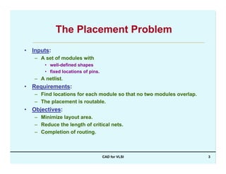
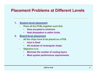
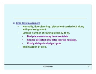
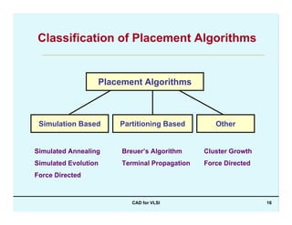
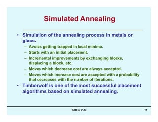
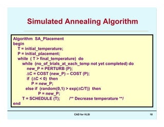
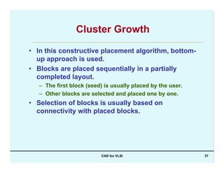
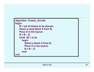
This document discusses placement in VLSI physical design. It defines placement as arranging modules on a layout surface with fixed shapes and pin locations. The key goals of placement are to minimize area, reduce critical net lengths, and ensure routability. Different placement problems are discussed at the system, board and chip levels. Common placement algorithms described include simulated annealing, genetic algorithms, and force-directed placement.