Downloaded 213 times


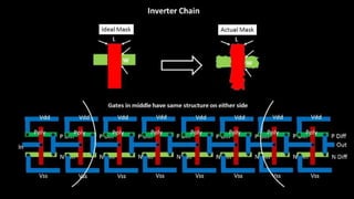

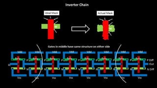

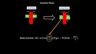


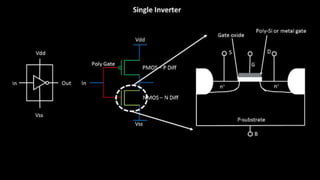

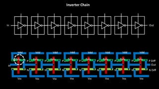
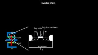

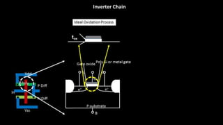

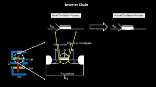

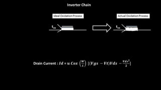
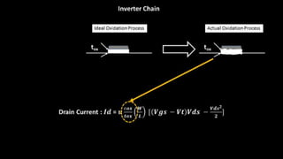


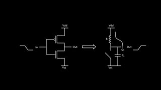
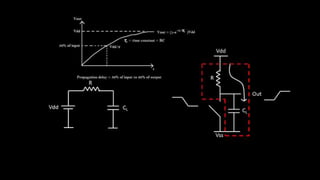

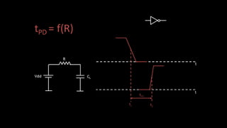

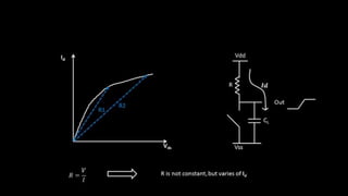
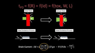

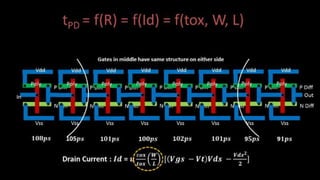

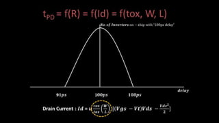
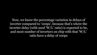
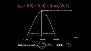
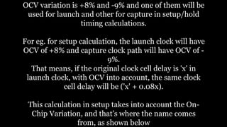
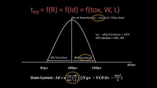


The document discusses on-chip variation (OCV) in static timing analysis, focusing on how variations during the etching and oxide thickness processes impact the performance of inverters in a clock path. It highlights the importance of modeling these variations in OCV calculations to assess how they affect drain current and propagation delay, which is crucial for ensuring proper timing in VLSI design. The author also shares personal experiences and resources related to circuit design and physical design flows.


![[Back2School] STA Methodology- Chapter 7pdf](https://cdn.slidesharecdn.com/ss_thumbnails/stamethodology-250624214856-5fd24ebc-thumbnail.jpg?width=640&height=640&fit=bounds)